[6] Handling Guide
101
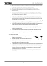
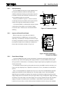
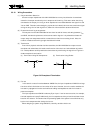
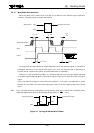
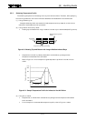
3.3.4 Input processing
Inputs to CMOS ICs have such a high impedance that
the logic level becomes undefined under open input
conditions. Should the floating input be neither High nor
Low, both P-channel and N-channel transistors turn on,
and unnecessary supply current flows.
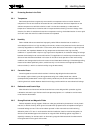
Therefore, as shown in Figure 3.1, be sure to connect
unused input lines to V
CC
, GND or other inputs and the
output to the logic level determined by the inputs.
In the case of CMOS, if a soldered part has poor contact,
a malfunction of the system or an increase in supply
current will occur. Therefore, care must be taken when
soldering.
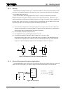
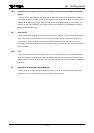
3.3.5 Inputs to a Printed Circuit Board
When the input pin of a printed circuit board is
connected directly to a CMOS input, that input floats
electrically. This condition is the same as a when a single
IC is being transported or stored. It is advisable, therefore,
to connect this input to V
CC
or GND via a resistance on
the printed circuit board, as shown in Figure 3.2.
3.3.6 Power Source Design
In general, CMOS has a small current consumption in comparison with bipolar digital ICs, and
therefore it only needs a low-capacity power supply. However, in practice CMOS consumes power
during transition, and therefore, it is necessary to keep the high-frequency impedance of the power
source at a low level.
It is advisable to make the wiring of the power source (V
CC
) and GND lines thick and short, and
insert, as a high-frequency filter, a capacitor of from 0.001 µF to 0.1 µF between V
CC
and GND for
each IC.
Also, it is recommended that a capacitor of from 10 µF to 100 µF be inserted between the power
supply input and GND as a low-frequency filter. The mean supply current varies considerably
depending upon the operating frequency of the system, the existence of capacitive load, the power
supply voltage and the rise and fall of the input signal. When using a simple power supply consisting
of a battery and a zener diode, if the mean supply current is high, please be careful with the power
supply, as its power is low. When there is overshoot or undershoot during the power supply’s
transition time use a filter or similar device so that the absolute maximum rating is not exceeded.
Figure 3.1 Treatment of Inputs
Figure 3.2 Input Processing by
Printed Circuit Board
V
CC
GND (※Unused gate)
※
※
R
R
R
V
DD
R:
∼
−
100 kΩ