PC Processors (Mobile Intel Pentium III-M)
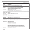
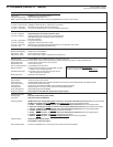
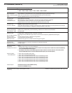
Code name
Instruction architecture
MMX™ / Streaming SIMD
Technology
L1 cache - bus
L1 cache - size/controller
L1 cache - write policy
L1 cache - organization
L2 cache - size
L2 cache - data path
L2 cache - buffering
L2 cache - organization
L2 cache - write policy
Frontside bus - speed
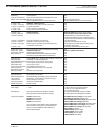
Memory addressability
System bus - width
System bus - parity
Execution units
Supscal dispatch/execute
Superscalar issue/retire
Out-of-order instructions
Branch prediction
Speculative execution
Math coprocessor
Serial number
Bus architecture
Internal processing
User registers
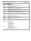
Cache line size
Power management
Multiple processors
Technology (micron)
Package type
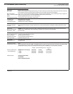
Frequency (MHz)
Chipset support
Server blade support
All trademarks are the property of their respective owners
© IBM Corp.
(18INTEL) Compiled by Roger Dodson, IBM. January 2003
Tualatin (pronounced "TWO-ala-tin")
IA-32 / CISC/RISC/micro-ops
MMX (57 new instructions) / Streaming SIMD Extensions (70 new instructions)
Enhanced Intel SpeedStep™ technology
64-bit / full speed
16KB data; 16KB instruction / integrated / non-blocking
Write-back or thru (data); write-thru (instruction)
4 way set associative (data); 2 way set associative (instruction)
512KB / full speed (Advanced Transfer Cache) / integrated / unified (internal die; on die)
256-bit data path / quad-wide cache line / ECC
Intelligent buffering of read and stores (called Advanced System Buffering with 4 writeback buffers, 6 fill buffers,
8 bus queue entries) / Data Prefetch Logic
8-way set associative / non-blocking / pipelined burst synchronous
Write-through or write-back (programmable per line), uncacheable, write-protect
133MHz (some at 100MHz)
64GB memory addressability
64-bit system bus with ECC
ECC on system bus; parity on address bus (frontside bus)
2 integer/MMX units; 1 floating point unit; 1 load unit; 1 store unit
5 micro-ops per cycle (3 micro-ops is typical); Pipeline stages: decoupled, 14 stage superpipelined
Issues 6 micro-ops per cycle (3 micro-ops is typical) / retires 3 micro-ops per cycle
Yes (called dynamic execution)
Dynamic (based on history) / 512 entry BTB / typically predicts 10 to 15 nested branches
Yes (typically 20 to 30 instructions beyond counter with an average of 5 branches)
Pipelined math coprocessor
Unique processor serial number
Independent backside and frontside buses operate concurrently / Dual Independent Bus Architecture (DIB)
32-bits (300 bit internal bus width)
8 GPR, 8 FP, 8 FPscalar and SIMD, 40 more GPR via register renaming
32 bytes (8 bytes x 4 chunks); burst mode bus of addr-data-data-data
Quick Start, Deep Sleep, Deeper Sleep
No SMP support (2-way SMP for 800MHz Low Voltage for server blade systems with ServerWorks
®
ServerSet III LE)
0.13u (130-nanometer)
Micro-FCPGA (Flip-Chip Pin Grid Array) for socketable boards
Micro-FCBGA (Flip-Chip Ball Grid Array) for surface mount boards
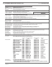
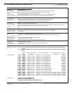
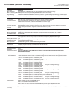
Frontside Maximum Performance Battery Optimized Announce
bus Mode Mode date
700MHz Ultra Low Voltage* 100MHz 700MHz at 1.1V 300MHz at 0.95V October 2001/Nov 2001*
733MHz Low Voltage 133MHz 733MHz at 1.15V 466MHz at 1.05V October 2001
750MHz Ultra Low Voltage 100MHz 750MHz at 1.1V 350MHz at 0.95V January 2002
750MHz Low Voltage 100MHz 750MHz at 1.15V 450MHz at 1.05V October 2001
800A MHz Low Voltage 100MHz 800MHz at 1.15V 500MHz at 1.05V October 2001
800MHz Low Voltage** 133MHz 800MHz at 1.15V 533MHz at 1.05V October 2001/Mar 2002**
800MHz Ultra Low Voltage* 100MHz 800MHz at 1.15V 400MHz at 1.05V April 2002*
800MHz Ultra Low Voltage* 133MHz 800MHz at 1.15V 400MHz at 1.05V April 2002*
850MHz Low Voltage 133MHz 850MHz at 1.15V 500MHz at 1.05V January 2002
850MHz Ultra Low Voltage 100MHz 850MHz at 1.1V 400MHz at 0.95V September 2002
866MHz Low Voltage 133MHz 866MHz at 1.15V 533MHz at 1.05V January 2002
866MHz 133MHz 866MHz at 1.40V 667MHz at 1.15V July 2001
866MHz Ultra Low Voltage 133MHz 866MHz at 1.1V 400MHz at 0.95V September 2002
900MHz Ultra Low Voltage 100MHz 900MHz at 1.1V 400MHz at 0.95V January 2003
933MHz Ultra Low Voltage 133MHz 933MHz at 1.1V 400MHz at 0.95V January 2003
933MHz Low Voltage 133MHz 933MHz at 1.15V 533MHz at 1.05V April 2002
933MHz 133MHz 933MHz at 1.40V 733MHz at 1.15V July 2001
1GHz 133MHz 1GHz at 1.40V 733MHz at 1.15V July 2001
1GHz Low Voltage 133MHz 1GHz at 1.15V 533MHz at 1.05V September 2002
1.06GHz 133MHz 1.06GHz at 1.40V 733MHz at 1.15V July 2001
1.13GHz 133MHz 1.13GHz at 1.40V 733MHz at 1.15V July 2001
1.2GHz 133MHz 1.2GHz at 1.40V 800MHz at 1.15V October 2001
1.26GHz 133MHz 1.2GHz at 1.40V 800MHz at 1.15V September 2002
1.33GHz 133MHz 1.2GHz at 1.40V 800MHz at 1.15V September 2002
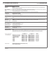
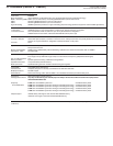
Intel 830MP, 830M, 830MG and others
* Supported in server blade systems; Micro-FCBGA only; uses Intel 440GX chipset
** Announced March 2002 for server blade systems; Micro-FCBGA only; supports 2-way SMP in server blade
systems with ServerWorks ServerSet III LE chipset
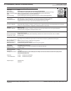
Mobile Intel
®
Pentium
®
III Processor-M for mobile systems (and server blade systems)
L2 cache bus also called Backside Bus
Memory or system bus also called
Frontside Bus
Created by IBM PC Institute
Personal Systems Reference (PSREF)


