


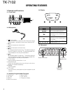

12
TK-7102
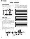
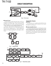
D10,12
Q11
TX VCO
Q15
BUFF
AMP
D9,11
Q10
RX VCO
Q7,12
T/R SW
Charge
pump
LPF
Phase
comparator
1/M
1/N
5kHz/6.25kHz
5kHz/6.25kHz
REF
OSC
16.8MHz
PLL
DATA
IC1 : PLL IC
Q3
RF AMP
Fig. 6 PLL circuit
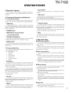
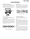
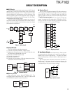
■ Unlock Circuit
During reception, the 8RC signal goes high, the 8TC sig-
nal goes low, and Q29 turns on. Q31 turns on and a voltage
is applied to the collector (8R). During transmission, the
8RC signal goes low, the 8TC signal goes high and Q30
turns on. Q33 turns on and a voltage is applied to 8T.
The CPU in the control unit monitors the PLL (IC1) LD
signal directly. When the PLL is unlocked during transmis-
sion, the PLL LD signal goes low. The CPU detects this
signal and makes the 8TC signal low. When the 8TC signal
goes low, no voltage is applied to 8T, and no signal is trans-
mitted.
IC6
CPU
Q29
SW
Q31
SW
IC1
PLL
Q30
SW
Q33
SW
LD
8RC
8C
8R 8T
8TC
PLL lock
: LD "H"
Fig. 7 Unlock circuit
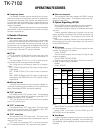
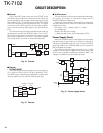
Q20
BUFFER
2SC4649
(N,P)
Q23
RF AMP
2SC3357
Q25
ANT
RF AMP
2SC2954
IC101
POWER AMP
M67741H-32
IC23
1/2
DIVIDER
UPB1509GV
IC3 Q11
D/A
CONVERTER
M62363FP
X1
TCXO
16.8MHz
VCO
2SK508NV
(K52)
IC1
PLL
MB15A02
Q15
BUFFER
2SC5108
(Y)
Q3
BUFFER
2SC4649
(N,P)
IC4
BUFFER
NJM2902V
IC6
IC3
MIC KEY
INPUT
CPU
784214GC
D/A
CONVERTER
M62363FP
IC3
D/A
CONVERTER
M62363FP
IC4
SUM AMP
NJM2902V
IC22IC21(1/2)MIC
MIC/IDC
NJM2100V
Splatter
FILTER
NJM2904V
Fig. 8 Transmitter system
Transmitter System
■ Outline
The transmitter circuit produces and amplifies the de-
sired frequency directly. It FM-modulates the carrier signal
by means of a varicap diode.
■ Power Amplifier Circuit
The transmit output signal from the VCO passes through
the transmission/reception selection diode (D19) and ampli-
fied to a specified level of the power module (IC101) by the
drive block (Q23 and Q25). The amplified signal goes to a
low-pass filter. The low-pass filter removes unwanted high-
frequency harmonic components, and the resulting signal is
goes the antenna terminal.
CIRCUIT DESCRIPTION