


14
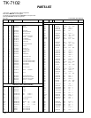
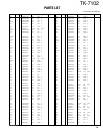
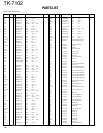
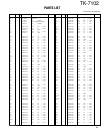
TK-7102
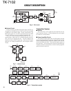
■ Encode
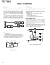
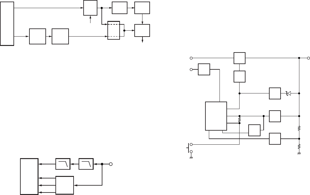
The QT and DQT signals are output from QT/DQT of the
CPU (IC6) and summed with the external pin DI line by the
summing amplifier (IC4) and the resulting signal goes to the
D/A converter (IC3). The DTMF signal is output from DTMF
of the CPU and goes to the D/A converter (IC3). The signal
is summed with a MIC signal by the summing amplifier
(IC4), and the resulting signal goes to the D/A converter
(IC3).
The D/A converter (IC3) adjusts the MO level and the bal-
ance between the MO and QT/DQT levels. Part of a QT/
DQT signal is summed with MO and the resulting signal
goes to the VCOMOD pin of the VCO. This signal is applied
to a varicap diode in the VCO for direct FM modulation.
■ D/A Converter
The D/A converter (IC3) is used to adjust MO modulation,
AF volume, TV voltage, FC reference voltage, and PC
POWER CONTROL voltage level.
Adjustment values are sent from the CPU as serial data.
The D/A converter has a resolution of 256 and the following
relationship is valid:
D/A output = (Vin – VDAref) / 256 x n + VDAref
Vin: Analog input
VDAref: D/A reference voltage
n: Serial data value from the microprocessor (CPU)
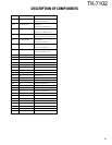
Power Supply Circuit
When the POWER switch on the display unit is pressed,
the power port on the display unit which is connected to
CPU port 18 (POWER), goes low, then CPU port 93 (SBC)
goes high, Q34 turns on, SB SW (Q42) turns on and power
(SB) is supplied to the radio.
This circuit has an overvoltage protection circuit. If a DC
voltage of 18 V or higher is applied to the power cable, D39
turns on and a voltage is applied to the base of Q38. This
voltage turns Q38 on and turns Q34 and SB off.
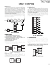
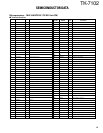
■ Decode
• QT/DQT/DTMF
The signal (DEO) passes through two low-pass filters of
IC11, goes to QTIN of the CPU (IC6) to decode QT, DQT.
The DTMF signal is decoded by a dedicated IC (IC9) and the
resulting signal is sent to the CPU (IC6) as serial data.
CIRCUIT DESCRIPTION
Fig. 14 Encode
Fig. 15 Decode
X1
TCXO
IC3
D/A
VCO
IC4
SUM
AMP
IC4
SUM
AMP
IC3
D/A
IC3
PLL
TCXO
MOD
VCO
MOD
HT
DI
QT/DQT
DTMF
IC6
CPU
IC6
CPU
IC11(2/2)
LPF
IC11(1/2)
LPF
QTIN
IC9
DTMF
DECO.
STD
SD
ACK
DEO
Q16
SW
Q42
SW
Q34
SW
Q38
SW
IC17
AVR
D39
B
IC15
RESET
SBC
IGN
INT
5M
IC6
CPU
POWER
SW
POWER
RESET
5M
Q18
INT
B
IGN
Fig. 16 Power supply circuit