


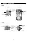
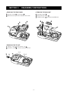
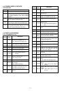
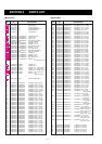

4 - 3
LINE
BATT
3V
+3V
R+3
T+3
DESCRIPTION
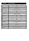
The voltage from the connected battery pack.
Common 3 V converted from the BATT line at
the 3V regulator circuit (IC6). The circuit outputs
the voltage regardless of the power ON/OFF
condition.
Common 3 V converted from the BATT line at
the +3V regulator circuit (Q25, D4).
Receive 3 V cotrolled by the R+3 regulator circuit
(Q18) using the “RXV” signal from CPU (IC1).
Transmit 3 V converted from the BATT line at the
T+3 regulator circuit (Q27, Q28, D5, etc.) using
the “TXV” signal coming from CPU (IC1).
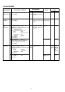
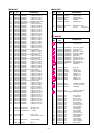
Outputs data signals to the PLL IC (RF
unit; IC1).
Outputs strobe signals for the PLL IC
(RF unit; IC1).
Outputs control signal for the +3V reg-
ulator circuit (MAIN unit; Q25, D4).
Output port for the CTCSS signals.
Outputs control signal for the MIC
amplifier (IC2).
Low : While microphone amplifier is
ON.
Input port for the CTCSS decode sig-
nals.
Input port for squelch level signal.
Input ports for the control signal from
the external remote microphone.
Input port form the connected battery
pack for low battery indication.
Input port for the RSSI signal from the
FM IF IC (RF unit; IC2) to detect receiv-
ing signal strength level.
Outputs clock signal to the EEPROM
(IC3).
Outputs data signals to the EEPROM
(IC3).
Output port for power save function,
applied to VCO regurator circuit (RF
unit; Q13, Q14, D8, D9).
Outputs the R+3 regulator control sig-
nal (Q18).
Outputs the T+3 regulator control sig-
nal (Q27, Q28, D5, etc.).
Outputs control signal for LCD back-
light.
Low : While LCD backlight is ON.
Outputs internal microphone control
signal.
High : While internal PTT switch is
pushed.
Outputs MIC mute signal for RING
function.
High : While RING signals are out-
put, etc.
51
52
53
54–56
57
58
59
60
61
62
73
74
75
76
77
78
79
80
PLLDA
PLLST
POWER
CTCO0–
CTCO2
TXMOD
CTCIN
SQLIN
REMIN
BATIN
SENIN
EEPCK
EEPDA
PSC
RXV
TXV
LAMPC
MICSW
MMUTE
Pin Port
Description
number name
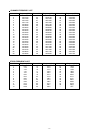
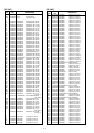
Input port for the PTT switch from the
external mic jack (MAIN unit; J1).
Low : External PTT switch is ON.
Input port for the internal PTT switch.
Low : While PTT switch is pushed.
Input port for the [DOWN] switch.
Input port for the [UP] switch.
Input port for the [MODE] switch.
Input port for the POWER switch.
Low : While POWER switch is
pushed.
Input port for PLL unlock signal from
the PLL IC (RF unit; IC1).
Low : During unlock.
Outputs beep audio signal.
Outputs volume mute switch (Q23)
control signal.
High : While squelched
Outputs control signal for the AF ampli-
fier regulator circuit (Q5, Q10, Q11).
High: When squelch is open.
Outputs clock signal to the PLL IC (RF
unit; IC1).
31
34
35
36
37
38
45
46
48
49
50
PTT2
PTT1
DOWN
UP
MODE
POWSW
UNLK
BEEP
RMUTE
AFON
PLLCK
Pin Port
Description
number name
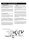
4-4 POWER SUPPLY CIRCUITS
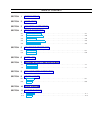
VOLTAGE LINE
4-5 PORT ALLOCATIONS
4-5-1 CPU (MAIN unit; IC1)