


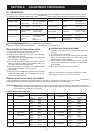
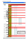
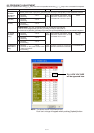

5 - 2
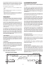
The processed AF signals from the base band IC (IC2) are
passed through the AF mute switch (IC8, pins 3, 4) and D/A
converter (IC6, pins 15, 16) for level adjustment. The level
adjusted AF signals are amplified by AF amplifier (IC22).
The amplified AF signals are then;
- Output from D-sub 25 pin connector (CONNECT UNIT;
J602).
or
- Buffer-amplified by Q49, then applied to connected micro-
phone via FRONT UNIT.
or
- Applied to the AF power amplifier (IC21, pin 1) to obtain AF
output power level, then applied to the internal/external
speaker via external speaker jack (J7).
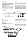
SQUELCH CIRCUITS
<NOISE SQUELCH>
The squelch mutes the AF output signals when no RF signals
are received. By detecting noise components (30 kHz and
higher signals) in the demodulated AF signals, the squelch
circuit toggles the AF power amplifi er ON and OFF.
A portion of the demodulated AF signals from the IF IC
(IC5, pin 9) are applied to the D/A converter (IC6, pin 1)
for level adjustment (squelch threshold adjustment). The
level-adjusted AF signals are output from pin 2 and passed
through the noise filter (IC5, pins 7, 8, R121−R124, C216
−C218). The filtered noise signals are amplified the noise
components only.
The amplifi ed noise components are converted into the pulse-
type signal at the noise detector section, and output from pin
13 as the “NOIS” signal. The “NOIS” signal is applied to the
CPU (IC14, pin 113), Then the CPU outputs signal “AFON2”
signal from pin 15 to the AF power amplifier controller (Q51,
Q52, D65), according to the “NOIS” signal level. The AF power
amplifi er controller toggles AF power amplifi er (IC21) ON and
OFF according to the “AFON” signal.
<TONE SQUELCH>
The tone squelch circuit detects tone signals and opens the
squelch only when receiving a signal containing a matched
sub audible tone. When the tone squelch is in use, and a
signal with a mismatched or no sub audible tone is received,
the tone squelch circuit mutes the AF signals even when the
noise squelch is open.
• CTCSS/DTCS
A portion of the demodulated AF signals are passed through
the active LPF (Q4, R45, R46, R47, R63, R64, C45, C46,
C47, C71) to filters CTCSS/DTCS signal. The filtered signal
is applied to the CPU (IC14, pin 64). The CPU compares the
applied signal and the set CTCSS/DTCS, then outputs con-
trol signal as same as “NOISE SQUELCH.”
• 2/5 TONE AND DTMF
2/5 tone signals in the demodulated AF signals are passed
through the LPF in the base band IC (IC2) and output from
pin 21, then applied to the CPU (IC14, pin 63) via tone
amplifer (IC1, pins 8, 9), and decoded.
5-2 TRANSMITTER CIRCUITS
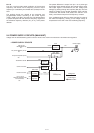
MICROPHONE AMPLIFIER CIRCUITS
The AF signals from the microphone (MIC signals) are
filtered and level-adjusted at the microphone amplifier
circuits.
AF signals from the connected microphone (MIC signals)
are passed through (bypassed) the ALC (Automatic Level
Control) amplifier (FRONT UNIT; IC505, pins 3, 5) via AF
switch (FRONT UNIT; IC507, pins 1, 6/7), then applied to
the microphone amplifier (FRONT UNIT; IC508, pin 3). The
amplified MIC signals are output from pin 4, and applied to
the MAIN UNIT.
The MIC signals from the FRONT UNIT are passed through
the Int./Ext. MIC switch (IC23, pins 1, 6), and applied to the
base band IC (IC2, pin 3) and processed.
The applied MIC signals are amplifi ed at the amplifi er (TXA1),
and level adjusted at the volume controller (VR1). The level
adjusted MIC signals are applied (bypassed) the compressor
section, pre-emphasis section, TX/RX HPF, de-scrambler, limiter,
splatter, in sequence, then applied to another volume controller.
The compressor compresses the MIC signals to provide high S/N
ratio for receive side, and the pre-emphasis obtains +6 dB/oct
audio characteristics. The TX/RX HPF filters out 250 Hz and
lower audio signals, the limiter limits its level and the splatter
filters out 3 kHz and higher audio signals. The filtered MIC
signals are level adjusted at another volume controller (VR2),
and then output from pin 7 via smoothing fi lter (SMF).
The MIC signals from the base band IC are passed through
the digital/analog switch (IC8, pins 12, 14), FM/PM switch
(IC3, pins 13, 14), and applied to the AF mixer (IC1, pin
13) where the MIC signals and tone signals are mixed with.
The mixed MIC signals are passed through D/A converter
(IC6, pins 3, 4) for level adjustment. The level adjusted MIC
signals are then applied to the VCO as modulation signals.
MODULATION CIRCUITS
The modulation circuits modulates the VCO oscillating signal
using the modulation signals.
The MIC signals from the microphone amplifier circuits are
applied to the D20 of TX VCO (Q19, D14, D17, D18, D20)
as the modulation signals, and modulate the VCO oscillating
signal by changing the reactance of D20.
The FM-modulated VCO output is amplified by buffer-
amplifiers (Q22, Q29), then applied to the power amplifiers
via D24 as the TX signal.
SIGNALING ENCODE
5/2-TONE, DTMF and CTCSS/DTCS signals are output
from the CPU (IC14) and passed through the LPF (IC7)
and level converter (IC6), then applied to the AF mixer
(IC1, pin 13) and mixed with MIC signals. The mixed tone
signals are passed through the D/A converter (IC6, pins 3,
4) for level adjustment. The level adjusted tone signals are
applied to the both of TX VCO (Q19, D14, D17, D18, D20)
and reference frequency oscillator (X1, pin 1) via the level
adjuster (IC1, pins 1, 3).
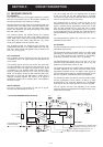
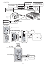
Scrambler/
De-scrambler
TX/RX
HPF
Pre-
emphasis
Limiter Splatter VR2
Expander
VR4
RXA2
SMF
De-
emphasis
Com-
pressor
VR1
(HPF)
RX
LPF
VR3
(HPF)
7 MOD
18
19
20
SIGNAL
3TXIN
• BASE BAND IC BLOCK DIAGRAM
23RXIN
21SDEC
TXA1
RXA1
BASE BAND IC (IC2)