


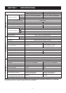
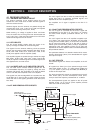
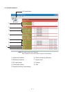
Loop
filter
Buffer
Q61
Buffer
Q3
Buffer
Q62
Buffer
Q71
to transmitter circuit
to 1st mixer circuit
D91
D92
5
8
Q51, D35–D39
TX VCO
Q41, D31–D34
RX VCO
IC1 MB15A02PFV
×2
30.6 MHz 2nd LO
signal to the FM IF IC
(IC231, pin 2)
Q221
Shift register
Prescaler
Phase
detector
Charge
pump
Programmable
divider
SCLK
PLSTBO
1
2
9
10
11
SDATAO
"LOINV" signal
to the CPU (IC661, pin 34)
LPF
PLL control signals
from D/A converter (IC251, pins 6–7)
15.3 MHz reference signal
from reference frequency osciilator (X1)
4 - 3
• PLL CIRCUITS
4-3 PLL CIRCUITS
4-3-1 GENERAL
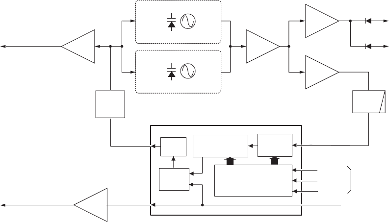
PLL circuits control TX and RX VCO circuits. IC1 is a
PLL IC and contains prescaler, programmable counter,
programmable divider, phase detector, charge pump in its
package.
The VCOs directly generate the transmit frequency and the
1st LO frequency for receiving. The PLL sets the divided
ratio based on the serial data from the CPU (IC661), and
compares the phase of the VCO output with the reference
oscillator's frequency (15.3 MHz) oscillated by X1.
If the oscillated signal drifts, the phase of its frequency
changes from the phase of the reference frequency, causing
a lock voltage change to compensate for the drift in the
oscillated frequency.
4-3-2 TRANSMIT LOOP
A portion of the generated signal at the TX VCO (Q51, D35–
D39) is applied to the PLL IC (IC1, pin 8) via buffer-amplifier
(Q71). The applied signal is divided at the prescaler section
and programmable divider section and is then applied to the
phase detector section.
The phase detector compares the input signal with the
reference frequency, and then outputs the control signal
(pulse-type) from pin 5 via the charge pump section. The
pulse-type signal is converted into DC voltage at the loop
filter (R17–R19, C16, C17), and then applied to the TX VCO
(Q51, D35–D39) as the lock voltage.
4-3-3 RECEIVE LOOP
The generated signal at the RX VCO (Q41, D31–D34) is
applied to the PLL IC (IC1, pin 8) via buffer-amplifier (Q71)
and is divided at the prescaler section and programmable
divider section and is then applied to the phase detector
section.
The phase detector compares the input signal with a
reference frequency, and then outputs the control signal
(pulse-type) from pin 5. The pulse-type signal is converted
into DC voltage at the loop filter (R17–R19, C16, C17), and
then applied to the RX VCO (Q41, D31–D34) as the lock
voltage.