


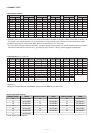
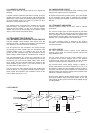
4 - 2
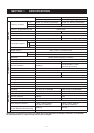
Power
AMP
APC
AMP
+
–
3
4
1
To ANT
TDETV
VCC
T1CON
RF signals
from TX/RX SW
T5V
D121
Pre-
drive
Buffer
AMP
ANT
SW
LPF
LPF
Q91
IC141
Q101
Q111
D132
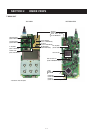
• APC CIRCUIT
4-1-6 SQUELCH CIRCUIT
Squelch circuit mutes AF output signal when no signals are
received.
A portion of the AF signals from the FM IF IC (IC231, pin 9) are
applied to the IC251 to control the level, and the active filter
(R239–R241, C237, C238). The filtered signals are applied to
the noise amplifier section in the FM IF IC (IC231, pin 8) to
amplify the noise components only.
The amplified noise components are detected at the noise
detector section, and output from pin 14 as the "NOISV"
signal to the CPU (IC661, pin 32). Then the CPU outputs
"AFMS" signal from pin 84 according to the "NOISV" signal
level to control the AF mute switch (Q411).
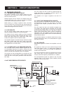
4-2 TRANSMITTER CIRCUITS
4-2-1 MIC AMPLIFIER, SPLATTER FILTER CIRCUITS
The MIC amplifier circuit amplifies audio signals from the
microphone within +6 dB/oct pre-emphasis characteristics
and amplifies to the level needed for modulation.
The AF signals from the microphone are passed through
the microphone switch (Q461) and the microphone mute
switches (IC682 A, pins 1, 2; IC682 B, pins 5, 6). The AF
signals are then passed through the pre-emphasis circuit
(R463, C463) to obtain frequency characteristics of +6 dB/oct.
The pre-emphasized AF signals are amplified at the
microphone amplifier (IC261 B), and adjusted its level at the
microphone gain control circuit (Q653, Q654, R474, R705,
R707, R708). The level adjusted signals are applied to the
limiter amplifier (IC491 A; pins 1, 2) to limit its level via the
AF mute switch (IC481 A; pins 1, 2).
The AF signals are then passed through the splatter filter
(IC491 B; pins 6, 7) to suppress unwanted 3 kHz and higher
audio signals, then applied to the modulation circuit via the
D/A converter (IC251; pins 3, 4).
4-2-2 MODULATOR CIRCUIT
The modulation circuit modulates the VCO oscillating signal
with the audio signals from the microphone.
AF signals from the D/A converter (IC251, pin 3) are applied
to the modulation circuit (D39) to modulate the oscillated
signal by changing the reactance of D39 at the TX VCO (Q51,
D35–38).
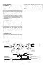
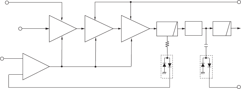
4-2-3 TRANSMIT AMPLIFIERS
Transmit amplifiers amplify the TX VCO output to transmit
power level.
The TX VCO output signal is buffer-amplified by the buffer
amplifiers (Q61, Q62) and passes through the TX/RX switch
(D91). The signals from the TX/RX switch are applied to the
another buffer amplifier (Q91), pre-drive (Q101) and power
amplifier (Q111) and amplified to the transmit level.
The power amplifier output is applied to the antenna
connector (J41: CHASSIS UNIT) via the antenna switching
circuit and the LPFs.
4-2-4 APC CIRCUIT
The APC (Automatic Power Control) circuit stabilizes
transmit output power and controls transmit output power
High, Middle and Low.
The RF output signal from the power amplifier (Q111)
is detected at the power detector (D121). The detector
converts the RF signals into DC voltage, and the detected
voltage is applied to the APC amplifier (IC141, pin 3).
The transmit output power setting voltage is applied to
another input terminal of the APC amplifier (IC141, pin 1) as
the reference voltage. The APC amplifier controls the bias of
the buffer, pre-drive and power amplifiers by comparing the
detected voltage and reference voltage. Thus the APC circuit
maintains a constant output power.
Another power detector (D132) detects the RF output level
and outputs "TDETV" signal to the CPU (IC661, pin 31). The
CPU outputs "TLED" signal to the LED driver (Q655) to light
TX LED (DS655).