


4 - 3
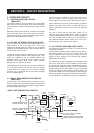
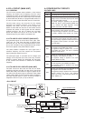
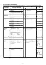
4-3 PLL CIRCUIT (MAIN UNIT)
4-3-1 GENERAL
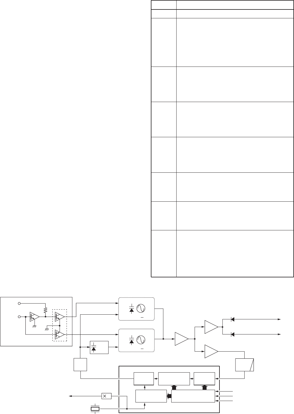
The PLL circuit provides stable oscillation of the transmit
frequency and receive 1st LO frequency. The PLL output
compares the phase of the divided VCO frequency to the
reference frequency. The PLL output frequency is controlled
by the divided ratio (N-data) of a programmable divider. IC1
is a PLL IC which controls both VCO circuit for TX and RX.
The PLL circuit, using a one chip PLL IC (IC1), directly
generates the transmit frequency and receive 1st IF
frequency with VCOs. The PLL sets the divided ratio
based on serial data from the CPU on the LOGIC unit and
compares the phases of VCO signals with the reference
oscillator frequency. The PLL IC detects the out-of-step
phase and output from the pin 6 for TX and RX. The
reference frequency (15.3 MHz) is oscillated at X1.
4-3-2 TX AND RX LOOP CIRCUITS (MAIN UNIT)
The generated signal at the TX-VCO circuit (Q51, D35
–D38, L34, L51, C32, C33, C52–C54) or RX-VCO (Q41,
D31–D34, L32, L41, C31, C41–C43) enters the PLL IC (IC1,
pin 8) and is divided at the programmable divider section
and is then applied to the phase detector section.
The phase detector compares the input signal with a
reference frequency, and then outputs the out-of-phase
signal (pulse-type signal) from pin 6.
The pulse-type signal is converted into DC voltage (lock
voltage) at the loop filter (R17–R19, C16–C19), and then
applied to varactor diodes (TX; D35–D38, RX; D31–D34)
of the TX-VCO and RX-VCO to stabilize the oscillated
frequency.
4-3-3 TX AND RX VCO CIRCUITS (MAIN UNIT)
The VCO circuit from Q41 (RX) and Q5 (TX) are buffer
amplified at the Q61 and Q62, and then sent to the TX/RX
swtich (D91, D92). The receive LO signal is applied to the
1st mixer circuit (Q191) through an attenuator (L203, R203
–R206, C202, C203), and the transmit signal is applied to
the buffer amplifier (Q91). A portion of the VCO output is
reapplied to the PLL IC (IC1, pin 8) via the Q71.
Shift register
Prescaler
Phase
detector
Loop
filter
FM
MOD.
Programmable
counter
Programmable
divider
X1
15.3 MHz
"2nd LO" signal (30.6 MHz)
to the FM IF IC (IC231, pin 2)
Q51, D35 D38
TX VCO
Buffer
Buffer
Buffer
Q62
D91
D92
Q71
Q61
11
10
9
PLSTBO
IC1 MB15A02PFV
SDATAO
SCLKO
to transmitter circuit
to the 1st mixer circuit
2
1
5
D39
8
LPF
Q41, D31 D34
RX VCO
2
Q82
Q81
VCOS
S5V
VCO SWITCH
Q221
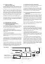
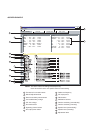
• PLL CIRCUIT
LINE
HV
VCC
CPU5V
M5V
R5V
T5V
V5V
S5V
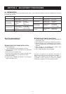
DESCRIPTION
The voltage from the attached battery pack.
The same voltage as the HV line (battery
voltage) which is controlled by the power switch
(VR unit; [OFF/VOL] control).
The output voltage is applied to the pre-drive
(MAIN unit; Q101), power amplifier (MAIN unit;
Q111), CPU5V and M5V regulator circuits
(LOGIC unit; IC551 and Q551–Q553).
Common 5 V converted from the VCC line by the
CPU5V regulator circuit (LOGIC unit; IC551).
The output voltage is applied to the CPU (LOGIC
unit; IC661), RESET circuit (LOGIC unit; IC581),
etc.
Common 5V converted from the VCC line by the
M5V regulator circuit (LOGIC unit; Q551–Q553).
The output voltage is applied to R5V, T5V, V5V and
S5V regulator circuits (LOGIC unit; Q322, Q323,
Q321 and Q561).
Receive 5V converted from the M5V line by the
R5V regulator circuit (MAIN unit; Q322).
The regulated voltage is applied to the 1st mixer
circuit (MAIN unit; Q191), RF and IF amplifiers
(MAIN unit; Q165, Q211).
Transmit 5V converted from the M5V line by the
T5V regulator circuit (MAIN unit; Q222).
The regulated voltage is applied to the buffer
amplifier (MAIN unit; Q91).
Common 5V converted from the M5V line by
the V5V regulator circuit (MAIN unit; Q321).
The regulated voltage is applied to the ripple
filter circuit (Q47).
Common 5V converted from the M5V line by the
S5V regulator circuit (LOGIC unit; Q561).
The regulated voltage is applied to the microphone
amplifier (LOGIC unit; IC471), limit amplifier
(LOGIC unit; IC491), LCD back light (LOGIC unit;
DS651–DS654), etc.
4-4 POWER SUPPLY CIRCUITS
VOLTAGE LINES