


TK-7102H
16
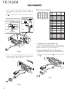
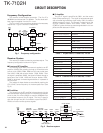
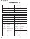
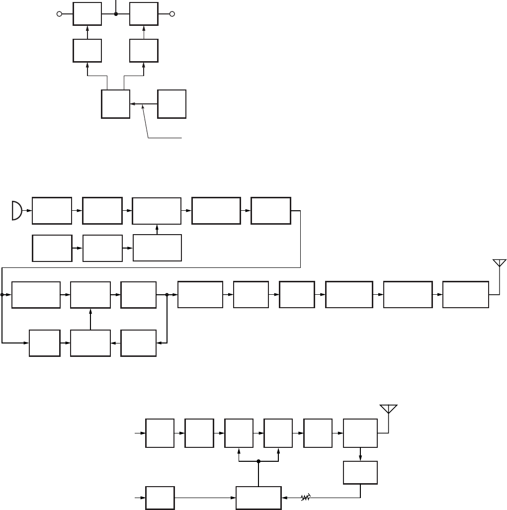
■ Unlock Circuit
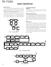
During reception, the 8RC signal goes high, the 8TC signal
goes low, and Q34 turns on. Q33 turns on and a voltage is
applied to the collector (8R). During transmission, the 8RC
signal goes low, the 8TC signal goes high and Q36 turns on.
Q35 turns on and a voltage is applied to 8T.
The CPU in the control unit monitors the PLL (IC401) LD
signal directly. When the PLL is unlocked during transmis-
sion, the PLL LD signal goes low. The CPU detects this sig-
nal and makes the 8TC signal low. When the 8TC signal goes
low, no voltage is applied to 8T, and no signal is transmitted.
IC101
CPU
Q34
SW
Q33
SW
IC401
PLL
Q36
SW
Q35
SW
LD
8RC
8C
8R 8T
8TC
PLL lock
: LD “H”
Fig. 7 Unlock circuit
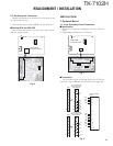
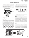
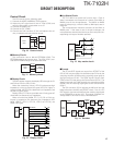
Transmitter System
■ Outline
The transmitter circuit produces and amplifies the desired
frequency directly. It FM-modulates the carrier signal by
means of a varicap diode.
■ Power Amplifier Circuit
The transmit output signal from the VCO passes through
the transmission/reception selection diode (D409) and ampli-
fied by Q501, Q502 and Q503. The amplified signal goes to
the final amplifier (Q504) through a low-pass filter. The low-
pass filter removes unwanted high-frequency harmonic com-
ponents, and the resulting signal is goes the antenna termi-
nal.
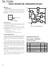
■ APC Circuit
The automatic transmission power control (APC) circuit
detects part of a final amplifier output with a diode (D606,
D607) and applies a voltage to IC501. IC501 compares the
APC control voltage (PC) generated by the D/A converter
(IC161) and DC amplifier (IC203) with the detection output
voltage. IC501 generates the voltage to control Q503 and
Q504 and stabilizes transmission output.
The APC circuit is configured to protect over current of
Q503 and Q504 due to fluctuations of the load at the antenna
end and to stabilize transmission output at voltage and tem-
perature variations.
RF
AMP
Q501
DRIVE
AMP
Q503
FINAL
AMP
Q504
PRE
DRIVE
AMP
Q502
DC
AMP
IC203
ANT
SW
D602~D605
LPF
ANT
POWER
DET
D606
D607
IC501
VR1
APC
CONTROL
D409
PC
IC161
3pin
Q411
RF AMP
2SC4649
(N,P)
Q501
RF AMP
2SC3357
Q502
PRE
DRIVE AMP
2SC3357
Q503
ANT
DRIVE AMP
PD55003TR
Q504
FINAL AMP
RD70HVF1
-01
IC402
1/2
DIVIDER
UPB1509GV
IC161 Q406
D/A
CONVERTER
M62363FP
X401
TCXO
16.8MHz
VCO
2SK508NV
(K52)
IC401
PLL
MB15A02
Q410
BUFFER
2SC5108
(Y)
Q404
RF AMP
2SC4649
(N,P)
IC203
BUFFER
NJM2902V
IC101
IC161
MIC KEY
INPUT
CPU
30622MAA
-B83GP
D/A
CONVERTER
M62363FP
IC161
D/A
CONVERTER
M62363FP
IC203
SUM AMP
NJM2902V
IC202IC201MIC
MIC/IDC
NJM2100V
Splatter
FILTER
NJM2904V
Fig. 9 APC circuit
Fig. 8 Transmitter system
CIRCUIT DESCRIPTION