CC2420
SWRS041B Page 28 of 89
0
0 A5 A4 A3 A2 A0A1 D
W
15 D
W
14 D
W
13 D
W
12 D
W
11 D
W
10 D
W
9 D
W
8 D
W
7 D
W
6 D
W
5 D
W
4 D
W
3 D
W
2 D
W
1 D
W
0
S7 S6 S5 S4 S3 S2 S0S1
0
1 A5 A4 A3 A2 A0A1
D
R
15 D
R
14 D
R
13 D
R
12 D
R
11 D
R
10 D
R
9 D
R
8 D
R
7 D
R
6 D
R
5 D
R
4 D
R
3 D
R
2 D
R
1 D
R
0S7 S6 S5 S4 S3 S2 S0S1
Read from register / RXFIFO:
Write to register / RXFIFO:
X
X
X X X
D
R
15
SCLK
CSn
SI
SO
SI
SO
t
sp
t
ch
t
sd
t
hd
t
ns
t
cl
1
A6 A5 A4 A3 A2 A0A1 B1 B0 0 X X X X X D
W
7 D
W
6 D
W
5 D
W
4 D
W
3 D
W
2 D
W
1 D
W
0
S7 S6 S5 S4 S3 S2 S0S1
1
A6 A5 A4 A3 A2 A0A1
D
R
7 D
R
6 D
R
5 D
R
4 D
R
3 D
R
2 D
R
1 D
R
0S7 S6 S5 S4 S3 S2 S0S1
Read one byte from RAM: (multiple reads also possible)
Read and write one byte to RAM: (multiple read / writes also possible)
X
X
X X X
D
R
7
B1 B0 1 X X X X XX
X
SI
SO
SI
SO
D
R
7 D
R
6 D
R
5 D
R
4 D
R
3 D
R
2 D
R
1 D
R
0 D
R
7
0
0 A5 A4 A3 A2 A0A1 D
W
7 D
W
6 D
W
5 D
W
4 D
W
3 D
W
2 D
W
1 D
W
0 D
W
7 D
W
6 D
W
5 D
W
4 D
W
3 D
W
2 D
W
1 D
W
0
S7 S6 S5 S4 S3 S2 S0S1
Write to TXFIFO:
X X X
SI
SO
S7 S6 S5 S4 S3 S2 S0S1 S7 S6 S5 S4 S3 S2 S0S1 S7
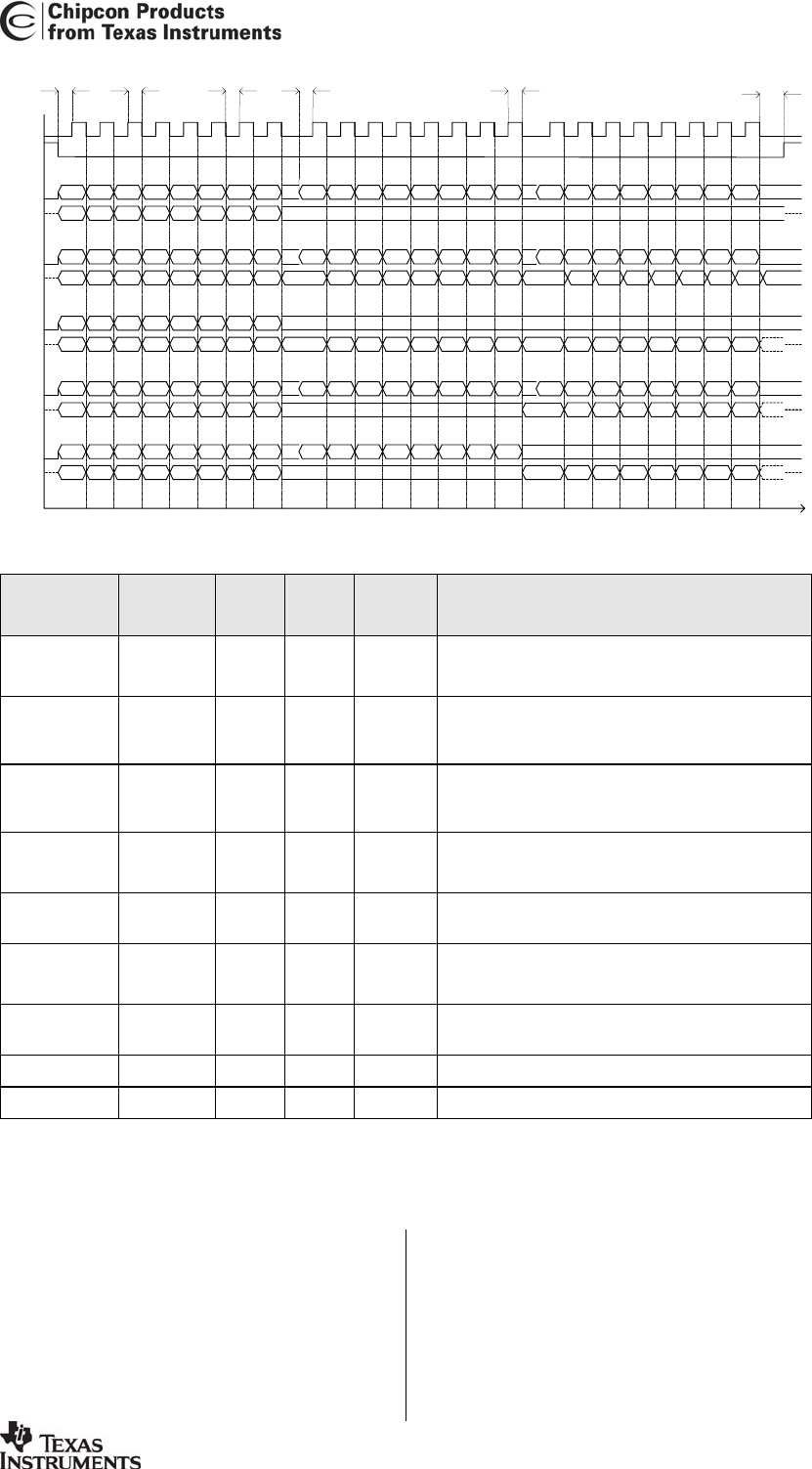
Figure 9. SPI timing diagram
Parameter Symbol
Min Max Units Conditions
SCLK, clock
frequency
F
SCLK
10 MHz
SCLK low
pulse
duration
t
cl
25 ns The minimum time SCLK must be low.
SCLK high
pulse
duration
t
ch
25 ns The minimum time SCLK must be high.
CSn setup
time
t
sp
25 ns The minimum time CSn must be low before the first
positive edge of SCLK.
CSn hold time t
ns
25 ns The minimum time CSn must be held low after the
last negative edge of SCLK.
SI setup time t
sd
25 ns The minimum time data on SI must be ready
before the positive edge of SCLK.
SI hold time t
hd
25 ns The minimum time data must be held at SI, after
the positive edge of SCLK.
Rise time t
rise
100 ns The maximum rise time for SCLK and CSn
Fall time t
fall
100 ns The maximum fall time for SCLK and CSn
Note: The set-up- and hold-times refer to 50% of VDD.
Table 4. SPI timing specification
13.3 Status byte
During transfer of the register access byte,
command strobes, the first RAM address
byte and data transfer to the TXFIFO, the
CC2420
status byte is returned on the SO
pin. The status byte contains 6 status bits
which are described in Table 5.
Issuing a SNOP (no operation) command
strobe may be used to read the status
byte. It may also be read during access to
chip functions such as register or FIFO
access.


