CC2420
SWRS041B Page 32 of 89
CSn
SI ADDRADDR
DATA
8MSB
DATA
8LSB
DATA
ADDR+1
SO
ADDR
TXFIFO
DATA
ADDR
DATA
ADDR+2
StatusStatus
- -
StatusStatus Status Status
Command
Strobe
Register
Read
TXFIFO
Write
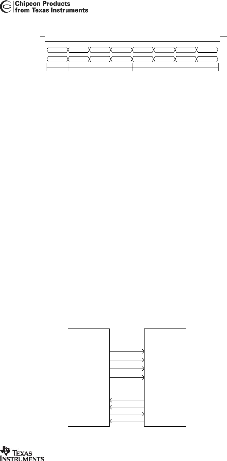
Figure 11. Multiple SPI Access Example
14 Microcontroller Interface and Pin Description
When used in a typical system,
CC2420
will
interface to a microcontroller. This
microcontroller must be able to:
Program
CC2420
into different modes,
read and write buffered data, and read
back status information via the 4-wire
SPI-bus configuration interface (SI, SO,
SCLK and CSn).
Interface to the receive and transmit
FIFOs using the FIFO and FIFOP
status pins.
Interface to the CCA pin for clear
channel assessment.
Interface to the SFD pin for timing
information (particularly for beaconing
networks).
14.1 Configuration interface
A
CC2420
to microcontroller interface
example is shown in Figure 12. The
microcontroller uses 4 I/O pins for the SPI
configuration interface (SI, SO, SCLK and
CSn). SO should be connected to an input
at the microcontroller. SI, SCLK and CSn
must be microcontroller outputs.
Preferably the microcontroller should have
a hardware SPI interface.
The microcontroller pins connected to SI,
SO and SCLK can be shared with other
SPI-interface devices. SO is a high
impedance output as long as CSn is not
activated (active low).
CSn should have an external pull-up
resistor or be set to a high level when the
voltage regulator is turned off in order to
prevent the input from floating. SI and
SCLK should be set to a defined level to
prevent the inputs from floating.
CC2420
C
CSn
SI
SO
SCLK
MOSI
MISO
SCLK
GIO2
FIFO
FIFOP
CCA
SFD
GIO0
Interrupt
GIO1
Timer Capture
Figure 12. Microcontroller interface example


