


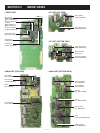
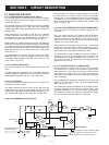
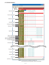

Loop
filter
X1
15.3 MHz
Q2, D5–D8
RX VCO2 (136–155 MHz)
Q1, D1–D4
RX VCO1 (155–174 MHz)
TX VCO
Q3, D10–D12
PLL control signals from the CPU (IC18)
PLL unlock signal
to the CPU (IC18, pin 73)
15.3 MHz
reference frequency signal
• PLL CIRCUIT
Buffer
Q4
Buffer
Q6
Buffer
Q5
to transmitter circuit
to 1st mixer circuit
D15
D14
BPF
PLST
SSO
SCK
4
11
6
10
14
15
16
PLL IC (IC1)
Shift register
Prescaler
Phase
detector
Divide
ratio
adjustment
Charge
pump
Programmable
divider
Reference
divider
#056
REGURATOR
6
REGURATOR
62%&
REGURATOR
36
REGURATOR
46
REGURATOR
26
REGURATOR
0OWERSWITCH
11
111
)#
)#
1
1
1
(6
6##
#056
#05
6
62%&
36
h3#v
6OLTAGELINE
#ONTROLSIGNAL
h4#v
h2#v
46
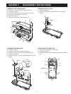
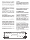
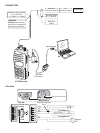
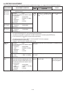
2ECEIVERCIRCUITS
!TTACHEDOPTIONALUNITS
!&LIFIERCONTROLLER
&2/.45.)411$
ETC
#05)#
%%02/-)#
ETC
0,,)#)#
"ASEBAND)#)#
ETC
0,,)#)#
4RANSMITTERCIRCUITS
26
48POWERAMPLIFIERS
2&5.)411
2&5.)4
112
#URRENT
SENSOR
)#
!TTACHEDOPTIONALUNITS
$!CONVERTERS
ETC
"ATTERYPACK
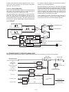
A portion of the each VCO output is applied to the PLL IC (IC1,
pin 6) via the buffer amplifi ers (Q4, Q5) and the tunable BPF
(D30, D31, L40, C170−C174).
5-3-2 PLL CIRCUIT (MAIN UNIT)
The PLL circuit provides stable oscillation of the transmit frequency
and receive 1st LO frequency. The PLL output frequency is
controlled by the divided ratio (N-data) from the CPU.
The buffer-amplifi ed VCO output signals from the tunable BPF
(D30, D31, L40, C170−C174) are applied to the PLL IC (IC1,
pin 6). The applied signals are divided at the prescaler and
programmable counter according to the “SSO” signal from the
CPU (IC18, pin 10). The divided signal is phase-compared with
the reference frequency signal from the reference frequency
oscillator (X1), at the phase detector.
The phase difference is output from pin 4 as a pulse type signal
after being passed through the internal charge pump. The output
signal is converted into the DC voltage (lock voltage) by passing
through the loop fi lter (R7, R9, R12, C17, C18, C20). The lock
voltage is applied to the variable capacitors (D1 and D2 of RX
VCO1, D7 and D8 of RX VCO2, D11 and D12 of TX VCO) and
locked to keep the VCO frequency constant.
If the oscillated signal drifts, its phase changes from that of
the reference frequency, causing a lock voltage change to
compensate for the drift in the VCO oscillating frequency.
5-4 POWER SUPPLY CIRCUITS (MAIN UNIT)
Voltage from the attached battery pack is routed to whole of the circuit in the transceiver via switches and regulators.
5 - 4