


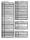

5-5-1 CPU (MAIN UNIT; IC18)
Pin
No.
Port
Name
Description
1 DSDA Outputs serial data to the D/A converter (IC20, pin 6).
2 DAST Outputs strobe signal to the D/A converter (IC4, pin 6).
3 SIDE3
Input port for [Side3] key (S4).
"Low"=When the key is pushed.
4−7 CBI0−3 Input ports for [ROTARY SELECTOR] (VR UNIT; S701).
10 SSO
Outputs serial data to the PLL IC (IC1, pin 15), D/A
converter (IC4, pin 8).
11 SCK
Outputs serial crock signal to the PLL IC (IC1, pin
14), D/A converter (IC4, pin 8).
13 PLST
Outputs PLL strobe signal to the PLL IC (RF UNIT;
IC1, pin 16).
15 DASW
Outputs mode (Digital/Analog) switching signal to
the D/A converter (IC14, pins 10, 11).
17 TMUT
Outputs transmit mute signal to the transmit mute
switch (RF UNIT; Q606).
18 NWC2
Outputs Narrow/Wide mode switching signal to the
bandwidth switches (Q26, D32, D33).
19 NWC1
Outputs Narrow/Wide mode switching signal to the
bandwidth switches (Q27, Q41, Q42, D34, D35).
20 DDSD
Outputs serial data to the DTMF decode IC (IC10,
pin 9).
21 DDAC
Outputs serial clock signal to the DTMF decode IC
(IC10, pin 11).
26 T5C
Outputs T5V line control signal to the T5V regulator
(Q15).
"Low"= While transmitting.
27 R5C
Output R5V line control signal to the R5V regulator
(Q16).
"Low"= While receiving.
28 S5C
Output S5V line control signal to the S5V regulator
(Q14).
"Low"=While power save mode.
29 PTTSW
Input port for [PTT] switch (S3).
"Low"=When the switch is pushed.
30 SIDE2
Input port for [Side2] key (S5).
"Low"=When the key is pushed.
32 RMUT Outputs mute signal to the AF mute switch (D42).
37 NOIS
Input port for the noise level from the FM IF IC (IC3,
pin 13).
38 POSW
Input port for power switch (VR UNIT; R702) from
power controller (D36).
39 DDST
Outputs strobe signal to the DTMF decode IC (MAIN
UNIT; IC10, pin 14).
40 MTCK
Outputs serial clock signal to the base band IC
(MAIN UNIT; IC5, pin 9).
41 PWON
Outputs VCC line control signal to the power switch
(Q30, Q31).
"Low"=While the power is ON.
43 SENC
Outputs single tone encode signal to the LPF (IC17,
pin 10).
44 BEEP Outputs beep sound to the AF circuits (IC4, pin 13).
45 SDEC Input port for decoded 2/5 tone and DTMF signals.
46 CDEC Input port for decoded CTCSS/DTCS signal.
47 ISENS
Input port for power amplifier current detect signal
from the current detector (RF UNIT; Q604, Q605).
48 BATV Input port for remaining battery power.
49 LVIN Input port for VCO lock voltage.
50 RSSI
Input port for RSSI signal from the FM IF IC (IC3,
pin 12).
55 EMER Input port for [Emer] switch (VR UNIT; S702).
Pin
No.
Port
Name
Description
70 CSFT
Outputs CPU clock frequency shift signal to the CPU
clock oscillator (X2, D38).
71 DUSE
Outputs CTCSS/DTCS select signal to the CTCSS/
DTCS switch (Q34).
73 UNLK
Input port for PLL unlock detect signal from the PLL
IC (IC1, pin 11).
74 RLED
Outputs RX indicator (VR UNIT; DS701) control
signal to the LED driver (VR UNIT; Q701).
75 TLED
Outputs TX indicator (VR UNIT; DS701) control
signal to the LED driver (VR UNIT; Q701).
78 FSDA
Outputs serial data to the expand IC (FRONT UNIT;
IC505, pin 3).
79 FSCL
Outputs serial clock signal to the expand IC (FRONT
UNIT; IC505, pin 3).
81 CIRQ
Input port for external connection detect signal from
J1 and J2.
88 SIDE1
Input port for [Side1] key (S6).
"Low"=When the key is pushed.
89−
91
CENC0−
2
Output CTCSS/DTCS signals to the LPF (IC17, pin 3).
92 EMPH
Outputs emphasis characteristic change signal to
the D/A converter (IC13, pins 9, 10).
93 MTDT Outputs serial data to the base band IC (IC5, pin 10).
96 MSCK
Outputs serial clock signal to the base band IC
(MAIN UNIT; IC5, pin 13).
97 PMFM
Outputs modulation mode switching signal to the
PM/FM switch (IC13, pin 11) .
98 ESDA Outputs serial data to the EEPROM (IC19, pin 5).
99 ESCL
Outputs serial clock signal to the EEPROM (IC19,
pin 6).
100 RESL Input port for reset signal from the reset IC (IC8, pin 1).
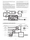
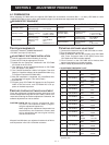
5-5-2 D/A CONVERTER (MAIN UNIT; IC20)
Pin
No.
Port
Name
Description
1T1
Outputs BPF tuning voltage to the tunable BPF (
D23,
D24, L31, L32, C120−C122, C125−C127
).
2T2
• While receiving
Outputs BPF tuning voltage to the tunable BPF
(
D28, D29, L33, L34, C140−C144, C147).
• While transmitting
Outputs TX power setting voltage to the APC
amplifi er (RF UNIT; IC601).
3 TXLVA
Outputs oscillation frequency adjust voltage to the
TX VCO (Q3, D10−D12).
4 RXLVA
Outputs oscillation frequency adjust voltage to the
RX VCO1/2 (
Q1, D1−D4/Q2, D5−D8).
5-5-3 EXPAND IC (FRONT UNIT; IC505)
Pin
No.
Port
Name
Description
4 AFON
Outputs AF power amplifi er (Q508, Q509) control
signal to the AF power amplifi er controller (Q501,
Q502, D508).
5 LIGH
Outputs backlight control signal to the backlight
driver (Q507−Q509).
6 SPCON
Outputs internal/external speaker select signal to
the SP/ESP switch (Q512, Q513).
7 MCON
Outputs internal/external microphone select signal
to the microphone controller (Q505, D504).
5 - 5
5-5 PORT ALLOCATIONS