


ASUS A7V133 User’s Manual64
4. BIOS SETUP
4. BIOS SETUP
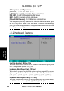
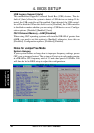
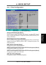
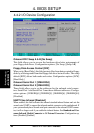
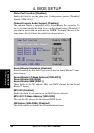
Chip Configuration
SDRAM Configuration [By SPD]
This sets the optimal timings for SDRAM related fields, depending on the
memory modules that you are using. Default setting is [By SPD], which
configures the subsequent 3 items by reading the contents in the SPD (Se-
rial Presence Detect) device. The EEPROM on the memory module stores
critical parameter information about the module, such as memory type, size,
speed, voltage interface, and module banks. Configuration options: [User
Define] [7ns(143MHz)] [8ns(125MHz)] [By SPD]
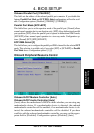
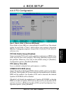
SDRAM CAS Latency
This controls the latency between the SDRAM read command and the time
that the data actually becomes available. NOTE: This field will only be ad-
justable when SDRAM Configuration is set to [User Define].
SDRAM RAS Precharge Time
This controls the idle clocks after issuing a precharge command to the
SDRAM. NOTE: This field will only be adjustable when SDRAM Con-
figuration is set to [User Define].
SDRAM RAS to CAS Delay
This controls the latency between the SDRAM active command and the
read/write command. NOTE: This field will only be adjustable when
SDRAM Configuration is set to [User Define].
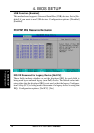
PCI Master Read Caching
Default: [Enabled] for Athlon Processors / [Disabled] for Duron Processors
Leave on default setting. Configuration options: [Disabled] [Enabled]
Delayed Transaction
Default: [Enabled] for Athlon Processors / [Disabled] for Duron Processors
Leave on default setting. Enabled, this frees the PCI Bus when the CPU is
accessing 8-bit legacy devices that normally consume about 50-60 PCI
Clocks without PCI delayed transaction. Select [Disabled] for legacy de-
vices that are not PCI 2.1 compliant. Configuration options: [Disabled] [En-
abled]
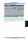
PCI to DRAM Prefetch [Enabled]
Configuration options: [Disabled] [Enabled]
Byte Merge [Enabled]
To optimize the data transfer on PCI, this merges a sequence of individual
memory writes (bytes or words) into a single 32-bit block of data. However,
byte merging may only be done when the bytes within a data phase are in a
prefetchable address range. Configuration options: [Disabled] [Enabled]
DRAM Read Latch Delay [Auto]
Configuration options: [-0.01 ns] [0.75 ns]...[Auto]