


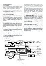
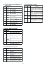

3 - 6
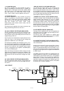
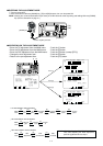
3-3 PLL CIRCUITS
3-3-1 GENERAL
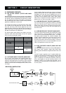
The PLL circuits generate a reference frequency (32.000
MHz); 1st LO frequencies (64.485–94.455 MHz); 2nd LO
frequency (64 MHz), 3rd LO frequency (433.000 kHz).
The 1st LO PLL adopts a mixer-less dual loop PLL system.
The BFO uses a DDS and a 2nd LO as a fixed frequency
double that the crystal oscillator.
3-3-2 1ST LO PLL (PLL UNIT)
The 1st LO PLL contains a main and reference loop as a
dual loop system.
The reference loop generates an approximate 10.5 MHz fre-
quency using a DDS circuit, and the main loop generates a
64.485 to 94.455 MHz frequency using the reference loop
frequency.
(1) REFERENCE LOOP PLL
The oscillated signal at the reference VCO (Q5301, D5301)
is amplified at the amplifiers (Q5302, Q5351) and is then
applied to the DDS IC (IC5101, pin 46). The signal is then
divided and detected on phase with the DDS generated fre-
quency.
The detected signal output from the DDS IC (pin 56) is con-
verted into DC voltage (lock voltage) at the loop filter
(R5136, R5146, C5112) and then fed back to the reference
VCO circuit (Q5301, D5301).
(2) MAIN LOOP PLL
The oscillated signal at one of the main loop VCOs (Q5521,
D5521, L5523) is amplified at the buffer amplifiers (Q5601,
Q5604) and is then applied to the PLL IC (IC5401, pin 6).
The signal is then divided and detected on phase with the
reference loop output frequency.
The detected signal output from the PLL IC (pin 2) is con-
verted into a DC voltage (lock voltage) at the loop filter and
then fed back to one of the VCO circuits (Q5521, D5521,
L5523).
The oscillated signal from the buffer amplifier (Q5601) is
also applied to the MAIN unit as a 1st LO signal after being
amplified at LO (Q5602) and buffer (Q5603) amplifiers or
passed through the bandpass filter (L5602–L5604,
C5610–C5616).
3-3-3 2ND LO AND REFERENCE OSCILLATOR
CIRCUITS (PLL UNIT)
The reference oscillator (X5251; [USA], [CAN], X5281;
[OTH]) generates a 32.0 MHz frequency for the DDS circuits
as a system clock and for the LO output. The oscillated sig-
nal is doubled at the doubler circuit (Q5202) and the 64.0
MHz frequency is picked up at the double tuned filter
(L5203, L5204). The 64.0 MHz signal is applied to the RF
circuit as a 2nd LO signal.
3-3-3 3RD LO CIRCUIT (PLL UNIT)
The DDS IC (IC5701) generates a 10-bit digital signal using
the 32 MHz system clock. The digital signal is converted into
an analog wave signal at the D/A converter (R5701–R5720).
The converted analog wave is passed through the bandpass
filter (L5781–L5783, C5781–C5785) and then applied to the
MAIN unit as the 3rd LO signal (433.000 kHz) via the atten-
uator (R5781–R5783).
Phase
detector
Programmable
divider
Programmable
divider
Loop filter
Doubler
DDS
DDS
DDS
DDS
D/A
convertor
D/A
convertor
Buff LO
Buff
Loop filter
Buff
PLL IC (IC5401)
MAIN loop VCO
Q5601 Q5602
Q5202
Q5801
Q5901
Q5302
Q5301, D5301
Q5351
Reference OSC. (32 MHz)
X5251; [USA], [CAN]
X5281; [OTH]
Reference loop VCO
IC5701
Q5882 Q5881
Q5603
Q5521,
D5521,
L5523
DDS IC
(IC5101)
LO
LO
AMP.
Buff
1st LO
(64–94 MHz)
2nd LO
(64 MHz)
DSC 2nd LO
(10.7103 MHz)
[USA], [CAN] only
DSC 1st LO
(12.8875–
27.5045 MHz)
[USA], [CAN] only
3rd LO
(443 kHz)
Phase
detector
Programmable
divider
Programmable
divider
• PLL CIRCUIT