


TH-K2AT/K2E/K2ET
13
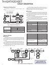
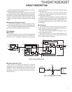
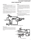
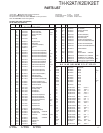
■ CTCSS/DCS
The encode signal is generated by the MPU (IC8) and output
from the TONE terminal (pin 41) of the MPU.
The unwanted high-frequency components of the encode
signal output from the MPU are removed with a low-pass filter,
and applied to VCO modulation input (MOD) and TCXO VC
terminal for modulation.
The VCO and TCXO modulation levels are adjusted by VR6
to produce flat modulation characteristics in low and high
ranges.
The decode signal is input to the SIGIN pin (pin 47) of the
MPU after the waveform of the audio signal from the FM IC is
rectified with a CTCSS/DCS filter (IC17). Then the set CTCSS
tone frequency and DCS code are detected by digital signal
processing in the MPU to control muting.
LPF
VR6
VCO
VOL OUT
MOD
X1
TCXO
VC
IC16
1
6
MIC
AMP
IC5
HPF
MIC
IC6
AF AMP
Vin
IC8
MPU
TONE
41
40
47
111
9
SIG INVOX IN
NOAA K, K2 types only
DTMF/BEEP
IC17D24Q30 IC3
CTCSS/DCS
FILTER
FM
IC
50
VR5
AMP
■ DTMF
The DTMF signal is generated by the MPU (IC8) and is
output from the DTMF/BEEP terminal (pin 40) of the MPU.
The DTMF signal is mixed with an audio signal at the input
side of the AF amplifier (IC6), and is output as a monitor tone.
The DTMF signal is mixed with a modulation signal at the
input side of pre-emphasis in the microphone amplifier (IC16)
and used as a transmit signal.
■ VOX
The IC5 and Q30 amplify the audio signal captured in the
microphone, and then the signal is converted into the DC
Voltage D24 rectifies.
The DC voltage activates the MPU (IC8), and the VOX starts.
■ Weather Alert (K and K2 types only)
The IC17 apmlifies the detected signal from the FM IC (IC3),
and the MPU (IC8) processes the signal. This signal processing
activates Weather Alert function.
Fig. 15 CTCSS/DCS, DTMF, VOX, Weather alert
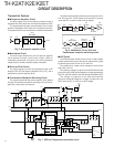
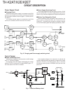
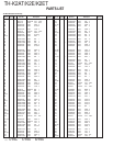
■ Serial Control
Serial control must be enabled from a transceiver menu so
that the REM/TXD pin of the speaker jack (J4) and the PTT
(RXD) pin of the microphone jack (J3) function as TXD and
RXD, respectively, when communicating with a personal
computer.
SP
POUT
10
HPF
IC5
IC6
AF AMP
PTTE
TXD
RXD
REM
IC8
MPU
SPK
AFO
SPG
REM/TXD
13
46
J4
SP JACK
IM
5MS
+
–
PTT
MIC
J3
MIC JACK
5MC
12
11
MIC
Fig. 16 Serial control
CIRCUIT DESCRIPTION