


TH-K2AT/K2E/K2ET
9
CIRCUIT DESCRIPTION
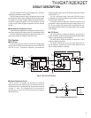
The APC voltage controls the gate voltage of Q11 and Q12,
and keeps transmission output stable.
The MPU detects power supply voltage and controls Q58
by transmission power supply voltage and transmission power.
For example, if the power supply voltage during transmission,
is equal to or higher than approx. 10.5 V and if power is at Mid
or Low level, the APC voltage level applied to Q12 is reduced
by Q58.
■ Temperature Protection Circuit
To prevent thermal destruction of the power amplifier (Q12),
this circuit reduces APC voltage when Q12 temperature rises.
The MPU (IC8) detects temperature with a thermistor (TH1)
and controls reference voltage to the APC circuit.
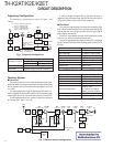
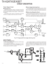
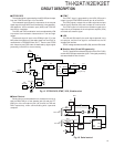
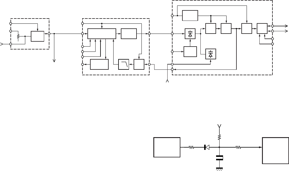
PLL System
■ PLL Circuit
A reference frequency of 5 kHz or 6.25 kHz is produced by
dividing the 12.8 MHz reference frequency of the TCXO (X1)
with PLL IC (IC1). Comparison frequency is produced by
TCXO
PLL IC
IC1
LOOP
FILTER
TO
TCXO
5C
5/0V
5MS
5/0V
PLL
5C
5/0V
VC
X1
12.8MHz
CLOCK
DATA
LE
Fo/LD
IF
Rectifier
LPF Q6
RF
Amp
D1,D2
VCO
5C
5/0V
LV
1~5V
SHIFT
H/L
Ripple
Filter
Q4
OSC
Q1
Buff
Amp
Q2
RF
Amp
Q5
SW
D8,D9
MOD
SHIFT
SW
Q3
MOD
12.8MHz
TX
RX
5T 5/0V
5R 5/0V
VR1
Fig. 8 PLL and VCO circuit
amplifying VCO output with an RF amplifier (Q6) and dividing
it with the PLL IC.
The PLL synthesizer with 5 kHz and 6.25 kHz step is
configured by comparing phases of the reference frequency
and comparison frequency.
The phase difference between reference frequency and
comparison frequency passes through a charge pump in the
PLL IC, then ripples are removed with a loop filter with low-
range passing characteristics to produce VCO control voltage
(lock voltage).
■ VCO Circuit
The VCO produces a desired frequency directly with a
Colpits oscillation circuit containing an oscillation transistor (Q1)
used for both transmission and reception.
The VCO control voltage is applied to varicap (D1, D2) to
produce a desired frequency.
The SHIFT terminal (pin 113) of the MPU (IC8) goes "H"
during reception, and the shift control switch (Q3) is turned
ON to change oscillation frequency.
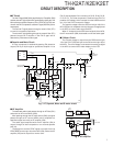
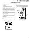
Fo/LD
PLL LD
IC8
MPU
IC1
PLL IC
R32
D16
C40
R35
14
102
5C
Fig. 9 Unlock detection circuit
■ Unlock Detection Circuit
When the PLL is unlocked, the waveform of the pulse
output from the Fo/LD terminal (pin 14) of the PLL IC (IC1) is
rectified with R32, D16, R35 and C40, and the Fo/LD terminal
is made “L” level. The voltage at the Fo/LD terminal is
detected by the MPU to control transmission/reception
switching timing.