


TH-K2AT/K2E/K2ET
8
CIRCUIT DESCRIPTION
Transmitter System
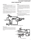
■ Microphone Amplifier Circuit
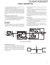
The audio signal from the microphone passes through a
high-pass filter (IC5) and enters a microphone amplifier (IC16).
The signal passes through a pre-emphasis circuit, limiter
amplifier and splatter filter inside the microphone amplifier.
The splatter filter will remove distortion outside the audio band.
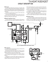
■ Modulation Circuit
The audio signal amplified by the microphone amplifier
(IC16) passes through a semi-fixed volume (VR5) for
modulation adjustment, and goes to the VCO modulation
varicap (D6) for variable reactance phase modulation.
■ Drive and Final Circuit
The output signal from VCO (Q1) passes through an RF
amplifier (Q2, Q5, Q9) and drive amplifier (Q10, Q11), and is
amplified by a power amplifier (Q12).
■ Transmission/Reception Switching Circuit
The signal amplified by the power amplifier (Q12) passes
through a transmission/reception switching circuit and a low-
pass filter, and is fed to the antenna.
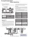
MIC IC5
HPF
IC16
MIC AMP
Pre-
emphasis
Splatter
filter
VCO
Limiter
61
Fig. 5 Microphone amplifier circuit
MIC
HPF
MIC
AMP
IC16
ANT
SW
D10,L19
D12,D13
VCO
Q1
LPF
IC5
VR5
MAX DEV
Q2
RF AMP
Q5
RF AMP
Q9
RF AMP
Q10
DRIVE AMP
Q11
DRIVE AMP
Q12
POWER AMP
ANT
Fig. 6 Modulation, Drive, Final and
Transmission/reception switching circuit
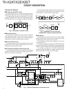
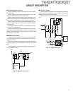
■ APC Circuit
The APC (Automatic Power Control) circuit is used to obtain
a stable transmission power and controls transmission output
by detecting the drain current of Q11 and Q12.
The transmission output can be changed in three levels:
High, Mid, and Low.
The reference voltage is output from the BPF/APC terminal
(pin 6) of the MPU (IC8) and the detection voltage generated by
R70, R71 and R72 are fed to the APC differential amplifier (IC2).
The voltage in proportion to the difference between
reference voltage and detection voltage is output from the
BOUT terminal (pin 7) of IC2 as an APC voltage.
Q10
Q15
Q11
Q12
VGG
Q58
VDD
LPF
ANT
D12
D13
RX
5T
B
1
AOUT
IC2
APC AMP
2
A–IN
3
A+IN
4
8
7
6
5
GND
V+
BOUT
B–IN
B+IN
R72
R71
R70
Q14
B
Q13
+
TH1
–t
Q55
7
KAPC
51
6
BPF/APC
THERM
16
FINAL
IC8
MPU
D10
L19
Fig. 7 APC and Temperature protection circuit
The transmission/reception switching circuit consists of D10,
L19, D12 and D13. These diodes are turned ON in transmit
mode and OFF in receive mode to switch signals.