


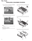
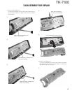
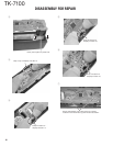
TK-7100
18
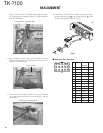
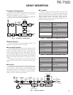
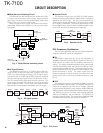
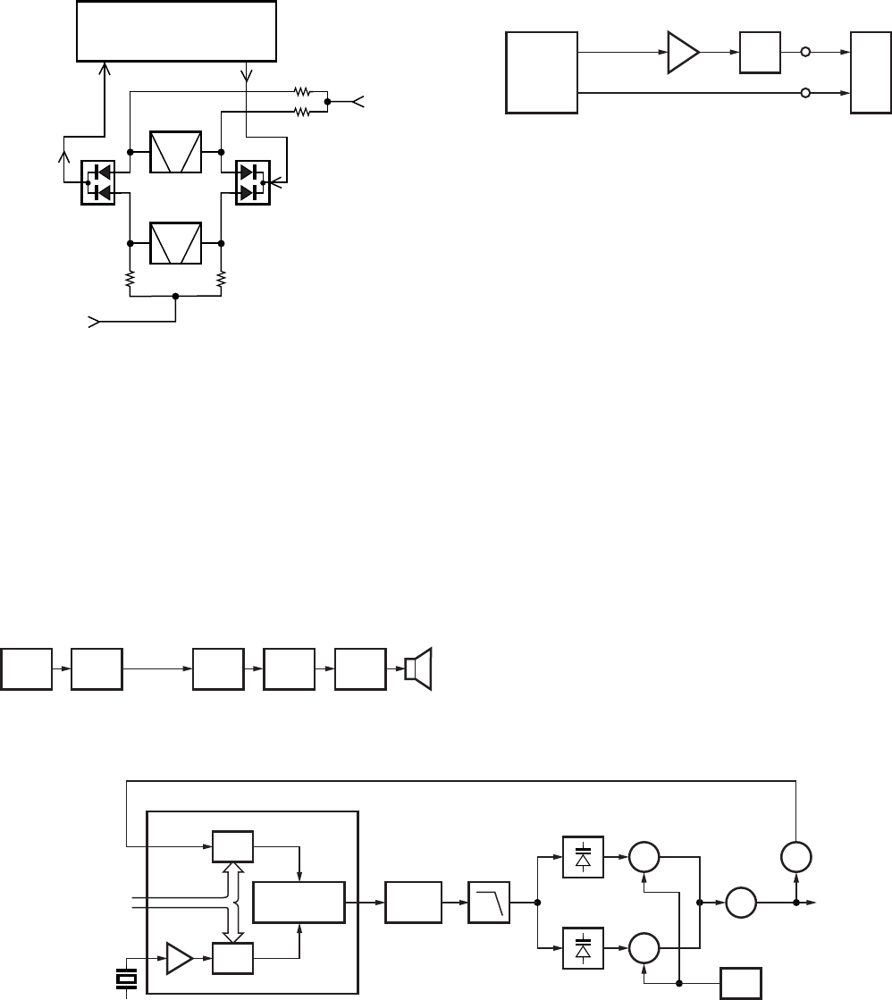
■ Wide/Narrow Switching Circuit
The Wide port (pin 65) and Narrow port (pin 64) of the CPU
is used to switch between ceramic filters. When the Wide
port is high, the ceramic filter SW diodes (D303, D302) cause
CF301 to turn on to receive a Wide signal.
When the Narrow port is high, the ceramic filter SW di-
odes (D303, D302) cause CF302 to turn on to receive a Nar-
row signal.
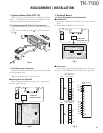
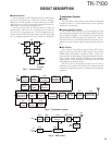
■ AF Signal System
The detection signal from IF IC (IC301) goes to D/A con-
verter (IC161) to adjust the gain and is output to AF filter
(IC251) for characterizing the signal. The AF signal output
from IC251 and the DTMF signal, BEEP signal are summed
and the resulting signal goes to the D/A converter (IC161).
The AFO output level is adjusted by the D/A converter. The
signal output from the D/A converter is input to the audio
power amplifier (IC252). The AF signal from IC252 switches
between the internal speaker and speaker jack (J1) output.
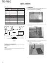
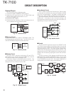
■ Squelch Circuit
The detection output from the FM IF IC (IC301) passes
through a noise amplifier (Q301) to detect noise. A voltage is
applied to the CPU (IC101). The CPU controls squelch ac-
cording to the voltage (SQIN) level. The signal from the RSSI
pin of IC301 is monitored. The electric field strength of the
receive signal can be known before the SQIN voltage is input
to the CPU, and the scan stop speed is improved.
Narrow
IC101 64pin
IF_IN MIX_O
IC301
IF System
CF302
(Narrow)
CF301
(Wide)
R320
R319
R317
R318
D303 D302
Wide
IC6 65pin
AF
Filter
D/A
CONV.
D/A
CONV.
IC161 IC251
IC161
W/NO
(EVOL2)
AF PA
IC252 SP
IF IC
IC301
Q301
NOISE AMP
D301IC301 IC101
AFO
RSSI
DET
CPU
IF
SYSTEM
SQIN
RSSI
Fig. 3 Wide/Narrow switching circuit
Fig. 4 AF signal system
Fig. 5 Squelch circuit
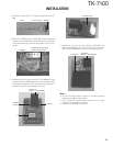
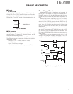
PLL Frequency Synthesizer
The PLL circuit generates the first local oscillator signal for
reception and the RF signal for transmission.
■ PLL
The frequency step of the PLL circuit is 5 or 6.25kHz. A
16.8MHz reference oscillator signal is divided at IC401 by a
fixed counter to produce the 5 or 6.25kHz reference fre-
quency. The voltage controlled oscillator (VCO) output signal
is buffer amplified by Q410, then divided in IC401 by a dual-
module programmable counter. The divided signal is com-
pared in phase with the 5 or 6.25kHz reference signal in the
phase comparator in IC401. The output signal from the
phase comparator is filtered through a low-pass filter and
passed to the VCO to control the oscillator frequency. (See
Fig. 6)
■ VCO
The operating frequency is generated by Q406 in transmit
mode and Q405 in receive mode. The oscillator frequency is
controlled by applying the VCO control voltage, obtained
from the phase comparator, to the varactor diodes (D405 and
D406 in transmit mode and D403 and D404 in receive mode).
The TX/RX pin is set low in receive mode causing Q408 and
Q407 to turn Q406 off, and turn Q405 on. The TX/RX pin is
set high in transmit mode. The outputs from Q405 and Q406
are amplified by Q410 and sent to the RF amplifiers.
D405,406
Q406
TX VCO
Q410
BUFF
AMP
D403,404
Q405
RX VCO
Q407,408
T/R SW
Charge
pump
LPF
Phase
comparator
1/M
1/N
5kHz/6.25kHz
5kHz/6.25kHz
REF
OSC
16.8MHz
PLL
DATA
IC401 : PLL IC
Q404
AMP
Fig. 6 PLL circuit
CIRCUIT DESCRIPTION