


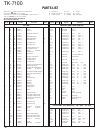
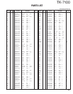
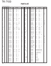
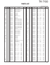
TK-7100
20
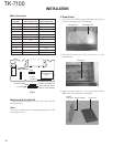
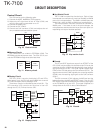
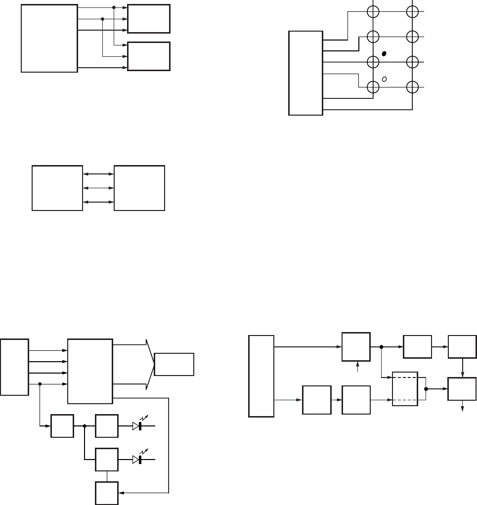
Control Circuit
The CPU carries out the following tasks:
1) Controls the WIDE, NARROW, TX/RX outputs.
2) Adjusts the AF signal level of the AF filter (IC251) and
turns the filter select compounder on or off.
3) Controls the display unit.
4) Controls the PLL (IC401).
5) Controls the D/A converter (IC161) and adjusts the vol-
ume, modulation and transmission power.
■ Memory Circuit
The transceiver has a 64k-bit EEPROM (IC66). The
EEPROM contains adjustment data. The CPU (IC101) con-
trols the EEPROM through three serial data lines.
IC161
D/A
converter
IC401
PLL
IC101
CPU
LD
DT
CK
PLLE
EEPCK
IC101
CPU
IC66
EEPROM
EEPDT
EEPWP
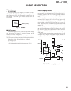
■ Display Circuit
The CPU (IC101) controls the display LCD and LEDs.
When power is on, the CPU will use the MBL line to control
the LCD illumination and key backlight LEDs.
The dimmer function is controlled by the switch Q11. The
LCD controller (IC2) controls the functions of the LCD
through the CE, CK, DI lines from the CPU.
■ Key Matrix Circuit
The TK-7100 front panel has function keys. Each of them
is connected to a cross point of a matrix of the KMI1 to KMO2
ports of the microprocessor. The KMO1 to KMO2 ports are
always high, while the KMI1 to KMI4 ports are always low.
The microprocessor monitors the status of the KMI1 to
KMO2 ports. If the state of one of the ports changes, the
microprocessor assumes that the key at the matrix point cor-
responding to that port has been pressed.
■ Encode
The QT and DQT signals are output from QT/DQT of the
CPU (IC101) and summed with the external pin DI line by the
summing amplifier (IC203) and the resulting signal goes to
the D/A converter (IC161). The DTMF signal is output from
DTMF of the CPU and goes to the D/A converter (IC161). The
signal is summed with a MIC signal by the summing amplifier
(IC203), and the resulting signal goes to the D/A converter
(IC161).
The D/A converter (IC161) adjusts the MO level and the
balance between the MO and QT/DQT levels. Part of a QT/
DQT signal is summed with MO and the resulting signal goes
to the VCOMOD pin of the VCO. This signal is applied to a
varicap diode in the VCO for direct FM modulation.
IC101
CPU
KMI1
KMI2
KMI3
KMI4
KMO2
KMO1
MON
SCN
VOL
UP
VOL
DN
CH
UP
CH
DN
X401
TCXO
IC161
D/A
VCO
IC203
SUM
AMP
IC203
SUM
AMP
IC161
D/A
IC401
PLL
TCXO
MOD
VCO
MOD
HT
DI
QT/DQT
DTMF
IC101
CPU
Fig. 10 Control circuit
Fig. 11 Memory circuit
Q10
SW
Q6
SW
IC101
CPU
D2~D5
Q9
SW
D19~D26,
D28~D31
Q11
SW
IC2
LCD
controller
CE
CK
DI
MBL
COM0~
COM3
SEG0~
SEG30
DIM
LCD
Fig. 12 Display circuit
Fig. 13 Key matrix circuit
Fig. 14 Encode
CIRCUIT DESCRIPTION