


3 - 4
detected voltage exceeds the power setting voltage. Then
the output voltage of the APC amplifier IC (IC1, pin 4) con-
trols the input current of the drive amplifier (Q4) and power
amplifier IC (IC2, pin 2) to reduce the output power.
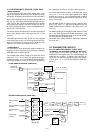
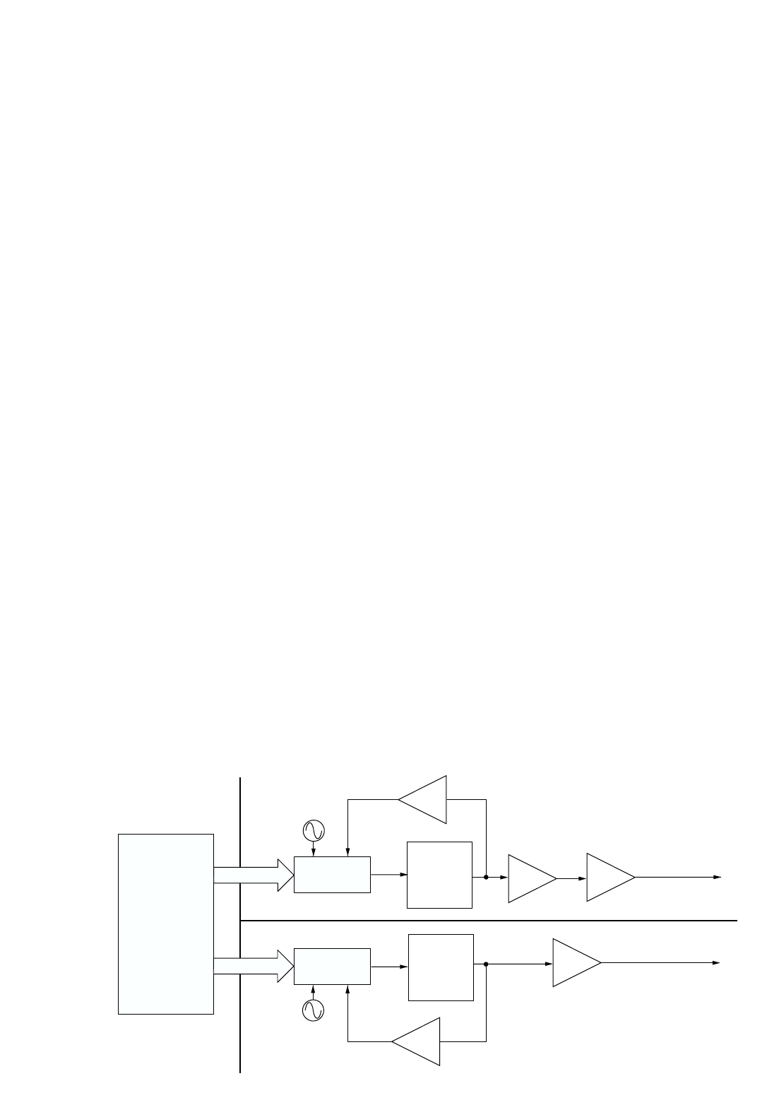
3-3 PLL CIRCUITS
3-3-1 GENERAL
Each receiver and transmitter circuit has an independent
PLL circuit for controlling frequencies. All PLL circuits are
shielded and installed on the RX and TX units.
PLL circuits steadily oscillate the transmit frequency and the
receive local frequency. The PLL output frequency is con-
trolled by divided ratio (N-data) of the programmable divider.
3-3-2 RECEIVER PLL CIRCUIT (RX UNIT)
The PLL IC (IC4) which includes in the prescaler, the pro-
grammable counter and the phase comparator generates
the 1st LO frequency with the VCO circuit (RVCO unit; Q1,
D1–D4). The PLL IC sets the divided ratio which bases on
N-data from the CPU (LOGIC unit; IC33) to control the pro-
grammable counter. The PLL IC compares a phases of the
VCO signal with the reference oscillator frequency, and is
then applied to the VCO circuit (RVCO unit; Q1, D1–D4).
3-3-3 RECEIVER REFERENCE OSCILLATOR
CIRCUIT (RX UNIT)
The 12.8 MHz reference frequency is produced by the oscil-
lator (X3). The frequency is adjusted by the D/A converter IC
(LOGIC unit; IC25). The reference frequency is applied to
the PLL IC (IC4, pin 1).
3-3-4 RECEIVER VCO CIRCUIT (RVCO UNIT)
The VCO circuit (Q1, D1–D4) generates the receive fre-
quency. The signal is applied to the buffer amplifier (Q2) and
is then applied to the PLL IC (RX unit; IC4). The signal is
amplified at the amplifiers (RX unit; Q8, Q9) and then pass-
es through the low-pass filter (RX unit; L23, L24, L39, L53,
C112–C114, C184, C216, C217) and attenuator (RX unit;
R81, R136, R137). The filtered signal is applied to the 1st
mixer circuit (RX unit; IC1) as 1st LO signal.
A part of the signal is applied to the PLL IC (RX unit; IC4) via
the amplifier (RX unit; Q14) as RX PLL lock voltage.
3-3-5 TRANSMITTER PLL CIRCUIT (TX UNIT)
The PLL IC (IC2) which includes in the prescaler, the pro-
grammable counter and the phase comparator. The PLL IC
sets the divided ratio which bases on N-data from the CPU
(LOGIC unit; IC33) to control the programmable counter.
The PLL IC compares a phases of the VCO signal with the
reference oscillator frequency, and is then applied to the
VCO circuit (TVCO unit; Q1, D1–D4).
3-3-6 TRANSMITTER REFERENCE OSCILLATOR
CIRCUIT (TX UNIT)
The 12.8 MHz reference frequency is produced by the oscil-
lator (X1). The frequency is adjusted by the D/A converter IC
(IC5, pin 14). The reference frequency is applied to the PLL
IC (IC2, pin 1).
3-3-7 TRANSMITTER VCO CIRCUIT (TVCO UNIT)
The VCO circuit (Q1, D1–D4) generates the transmit fre-
quency. The signal is applied to the buffer amplifier (Q2) and
is then applied to the amplifier (TX unit; Q1). The amplified
signal is applied to the PA unit.
A part of the signal is applied to the PLL IC (TX unit; IC2) via
the amplifier (TX unit; Q3) as TX PLL lock voltage.
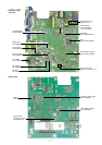
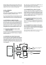
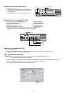
• PLL CIRCUITS
To the PA unit
To the 1st mixer circuit
AMP
AMP
AMP
PLL IC
PLL IC
RVCO
TVCO
AMP
AMP
X1
X3
CPU; IC33
TX UNIT
RX UNIT
LOGIC UNIT
DATA BUS
DATA BUS
D1–D4
Q1
D1–D4
Q1
Q14
Q8
Q9
Q1
Q3
IC2
IC4