


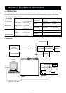

3 - 5
3-4 OTHER CIRCUITS
3-4-1 TELEPHONE IF CIRCUIT (LOGIC UNIT)
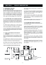
The signals from the telephone line (FRONT, J13) are
applied to the ringer detect circuit (IC48, D1, D5, R131,
R143, R145, C100, C103, C375). The detected signals are
applied to the CPU (IC33, pin 73) via “RING” line. The
“HOOKC” signal from the CPU (IC33, pin 72) and the “DP”
signal from IC47 are applied to the hook switch (RL1, RL2)
to off-hook.
Received AF signals from the RX unit pass through the high-
pass filter (IC9, pins 5, 7, 12, 14), de-emphasis (IC9, pins 1,
2) and low-pass filter circuits (IC10, pins 1, 3, 5, 7, 8, 9). The
filtered AF signals are amplified at IC7 (pins 12, 14) and are
then applied to the network IC (IC46, pin 16) via T6. The out-
put signals from IC46 are applied to the J13 (FRONT unit)
via L1, L2.
AF signals from J13 (FRONT unit) are applied to the network
IC (IC46, pins 8, 9). The output signals from IC46 (pins 8, 9)
are applied to the AF amplifier IC (IC1, pins 1, 2) via T8.
Amplified signals pass through the MIC mute switch (IC1,
pins 3, 4), the MIC mixer amplifier (IC2, pins 13, 14), the pre-
emphasis circuit (IC2, pins 8, 9), the high-pass filter circuit
(IC2, pins 1, 2, 6, 7), limiter amplifier circuit (IC3, pins 1, 2),
S-mixer circuit (IC3
,
, pins 6, 7), and splatter filter circuit (IC4,
pins 1, 3, 5, 7, 8, 10). The filtered signals are applied to the
TX unit.
After off-hook condition, DTMF signal from telephone line is
applied to the decoder IC (IC31) to decode the DTMF signal.
The DTMF signal is applied to the CPU (IC33) via serial sig-
nal line.
The clear down signal is detected at IC45 and is then
applied to the CPU (IC33). The “HOOKC” signal from the
CPU (IC33, pin 72) and the “DP” signal from IC47 are
applied to the hook switch (RL1, RL2) to on-hook.
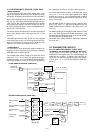
3-4-2 EEPROM CIRCUIT (LOGIC UNIT)
The detector IC (IC34) detects power supply ON-OFF volt-
age. The signal from IC34 is applied to IC33 (CPU). IC35,
IC36 are reset signal circuit which stabilizes memory data
for the EEPROM (IC37).
EEPROM (IC37) memories clone data and adjust setting
condition data.
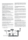
3-4-3 TEMPERATURE DETECT CIRCUIT
(LOGIC UNIT)
The temperature detect circuit protects the power amplifier
and power supply circuit from high temperature and stabi-
lizes the output power.
Inside temperature of the PA unit is detected at D15 (PA unit)
and is then applied to the amplifier IC (PA unit; IC3). The
amplified signal is applied to the CPU (IC33) to analyze the
temperature via IC32.
Inside temperature of the REG unit is detected at D6 (REG
unit) and is then applied to the amplifier (REG unit; IC9). The
amplified signal applied to the CPU (IC33) to analyze the
temperature via IC32.
IC32 selects “PATEMP” or “REGTEMP” signals from the PA
or REG unit.
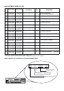
Description
The voltage from the DC power unit (CHASSIS;
EP1).
The same voltage as the PS 15V line which is
controlled by the power switch.
Common 9 V for converted from the VCC1 line
by the M9V regulator circuit (REG unit; IC1, Q8,
Q9). The voltage is applied to the TX and RX
units.
Common 9 V converted from the VCC1 line by
the L9V regulator circuit (REG unit; IC2).
Common 5 V converted from the L9V line by the
A5V regulator circuit (REG unit; IC3).
Common 5 V converted from the L9V line by the
L5V regulator circuit (LOGIC unit; IC38, Q48,
D43).
Common 5 V converted from the L9V line by the
C5V regulator circuit (LOGIC unit; IC38, Q45,
D13).
Common 5 V converted from the M9V line by the
TEL5V regulator circuit (LOGIC unit; IC11).
Line
PS 15V
VCC1
M9V
L9V
A5V
L5V
C5V
TEL5V
3-5 POWER SUPPLY CIRCUITS
3-5-1 LOGIC AND REG UNITS VOLTAGE LINES
Description
Transmit 5 V converted from the M9V line by the
T5V regulator circuit (TX unit; IC1).
Transmit 6 V converted from the M9V line by the
T6V regulator circuit (TX unit; IC4).
Common 9 V converted from the M9V line by the
V9V regulator circuit (TX unit; Q6).
Line
T5V
T6V
V9V
3-5-3 TX UNIT VOLTAGE LINES
Description
Common 5 V converted from the M9V line by the
+5V regulator circuit (RX unit; IC3).
Common 6 V converted from the M9V line by the
+6V regulator circuit (RX unit; IC7).
Receive 5 V converted from the R9V line by the
R5V regulator circuit (RX unit; IC6).
Receive 9 V controlled by the R9V regulator cir-
cuit (RX unit; Q15) using “R9C” signal from IC39
(LOGIC unit).
Common 9 V converted from the M9V line by the
V9V regulator circuit (RX unit; Q24).
Line
+5V
+6V
R5V
R9V
V9V
3-5-2 RX UNIT VOLTAGE LINES