


4 - 5
4-2-5 APC CIRCUIT (RF UNIT)
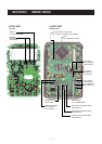
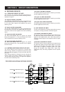
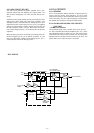
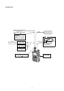
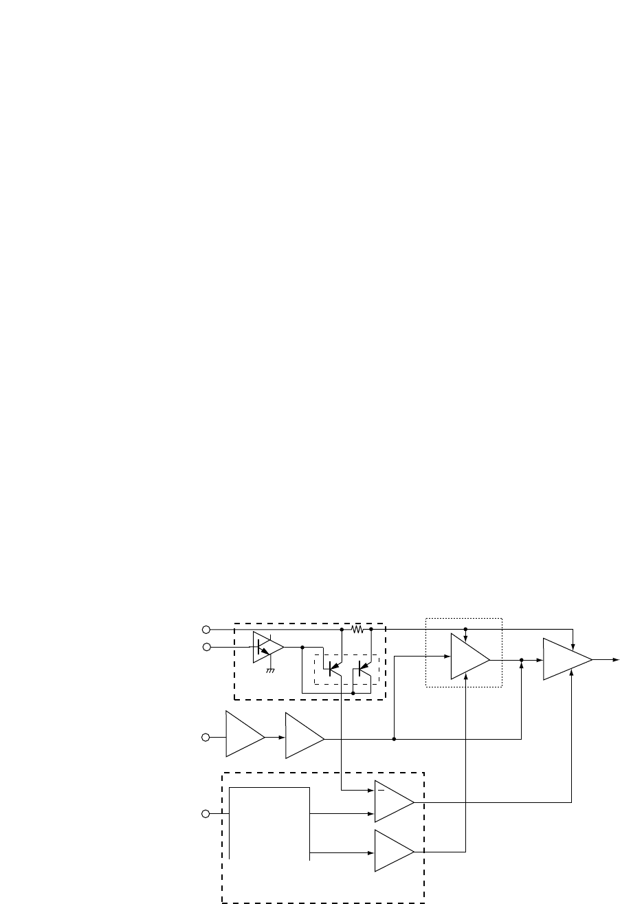
The APC circuit protects the power amplifier from a mis-
matched output load and stabilizes the output power. The
APC circuit is designed to use VHF and UHF bands com-
monly.
The APC sensor (R109) detects driving current from the drive
voltage at the drive (Q52) and power (Q51) amplifiers. The
detected current is converted into DC voltage at Q101, then
applied to the APC control circuit (IC101, pin 2). The applied
voltage is compared with a “PSET” voltage from the CPU via
the D/A convertor (IC251), and the APC control circuit out-
puts control voltage from pin 1 to control the drive and power
amplifiers.
When the driving current is increased, input voltage of the dif-
ferential amplifier (IC101, pin 2) will be increased. In such
cases, the differential amplifier output voltage (IC101, pin 1)
is decreased to reduce the driving current.
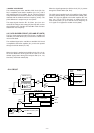
4-3 PLL CIRCUITS
4-3-1 GENERAL
A PLL circuit provides stable oscillation of the transmit fre-
quency and the receive local frequency. The PLL circuit
compares the phase of the divided VCO frequency to the ref-
erence frequency. The PLL output frequency is controlled by
the divided ratio (N-data) of a programmable divider.
4-3-2 144 MHz AND 430 MHz VCO CIRCUITS
(VCO UNIT)
• 144 MHz VCO CIRCUIT
The oscillated signal at the 144 MHz VCO circuit (Q1–Q3,
D1, D2) is amplified at two buffer amplifiers (Q7, Q11), and is
then applied to the PLL IC (IC201, pin 19). The signal is divid-
ed by serial data from the CPU (LOGIC unit; IC1) and phase
detected with the divided reference frequency (5 kHz). The
phase difference is output from pin 5 as pulses.
Q102
Q101
TXC
VCC
R109
APC SENSOR CIRCUIT
D/A CONVERTER
IC251
(RF unit)
+3
from Tx/Rx
switch
IC101
+
IC101
Differential
amplifier
1
7
2
36
PSET
514 DSET
VGGC
Pre
drive
Buff.
amp.
Power
amp.
Drive
amp.
Q52
IC51
Q54
Q51
to the antenna
50 MHz
RF transmit signal
144, 430 MHz
RF transmit signal
• APC CIRCUIT