


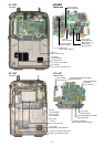
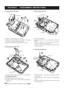

4 - 7
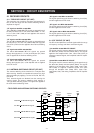
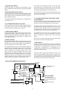
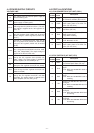
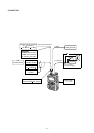
LINE
HV
VCC
CPU3
+3C
+3
+10V
AFV
R3
R3V
T3
DESCRIPTION
The voltage from the external power supply or
attached battery pack.
The same voltage as the “HV” line (external
power supply or battery pack).
Common 3 V converted from the “VCC” line by
CPU3 regulator IC (LOGIC unit; IC141). The out-
put voltage is supplied to the +3C regulator cir-
cuits, etc.
Common 3 V converted from the “VCC” line by
the +3C regulator circuit (LOGIC unit; Q142 and
Q145) using the +3CPU regulator (LOGIC unit;
IC141.)
Common 3 V converted from the “VCC” line by
the +3 regulator circuit (LOGIC unit; Q8 and Q9)
using the +3C regulator (LOGIC unit; Q142 and
Q145).
Common 10 V converted from the “+3” line by
the +10 regulator circuit(LOGIC unit; IC91, IC92,
Q91, D91, D300–D302). The output voltage is
applied to the RF and VCO units.
6 V for receiver circuit converted from the “VCC”
line by the “AF” regulator circuit (LOGIC unit;
Q201, Q202). The output voltage is applied to
the AF amplifier (AF unit; IC252, pin 2).
3 V for receiver circuit converted from the “+3”
line by the “R3” regulator circuit (RF unit; O353).
3 V for the receiver circuit converted from the
“VCC” line by the “R3V’ regulator circuit (AF unit;
Q208 and Q209).
3 V for transmitter circuit converted from the “+3”
line by the “T3” regulator circuit (RF unit; Q56
and D20). The output voltage is applied to the
buffer amplifier (RF unit; IC51, pin 6).
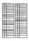
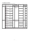
4-4 POWER SUPPLY CIRCUITS
VOLTAGE LINE
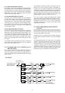
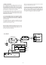
Pin Port
Description
number name
4
5
6
7
14
15
BSFT
B1C
B2C
B3
B4C
B5
Outputs frequency shift control signal
to tuned bandpass filters (RF unit).
Outputs 0.5–29.995 MHz band control
signal.
Low: While 0.5–29.995 MHz band is
receiving.
Outputs 30–75.995 MHz band control
signal.
Low: While 30–75.995 MHz band is
receiving.
Outputs 76–229.995 MHz band con-
trol signal.
Low: While 76–229.995 MHz band is
receiving.
Outputs 230–629.995 MHz band con-
trol signal.
Low: While 230–629.995 MHz band
is receiving.
Outputs 630–999.995 MHz band con-
trol signal.
Low: While 630–999.995 MHz band
is receiving.
Pin Port
Description
number name
5
6
11
12
13
14
Outputs frequnecy setting D/A data to
the reference oscillator (RF unit; X1).
Outputs the power amplifier’s output
power setting data to the APC con-
troller (RF unit; IC101).
Outputs D/A data to the tuned band-
pass filters (RF unit).
Outputs the R3 regulator (RF unit;
Q353) control signal.
High: While receiving.
Outputs attenuator control signal.
Low: Attenuator is ON.
Outputs the drive amplifier’s output
power setting data to the APC con-
troller (RF unit; IC101).
FSET
PSET
TUNE
RXC
ATT
DSET
4-5-2 R3V SWITCH IC (AF UNIT; IC51)
4-5 PORT ALLOCATIONS
4-5-1 D/A CONVERTOR IC (RF UNIT; IC251)