


TS-440
$
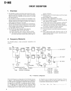
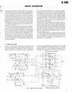
CIRCUIT DESCRIPTIO
N
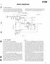
DSB by IC4 goes through the SSB transmit switching diode
s
D17 and D18, filter switching diodes D14 and D12, and SS
B
ceramic filter CF1, to obtain the SSB signal
. The SSB signa
l
then goes through the transmit switching diode D36 and i
s
fed into the transmit first mixer, IC6, where the SSB signa
l
is mixed with the output from the 8
.375 MHz oscillator i
n
the IF unit, and converted to 8
.83 MHz
. In CW or FM mode
,
the carrier signal from the PLL unit does not go through IC
5
BM or the 455 kHz filter
. These carrier signals are applie
d
to IC6 via switching diodes D53 and D54
. The output signa
l
from IC6 goes through the MCF to remove spurious compo
-
nents, and is amplified by the IF amplifier Q46 (3SK73) an
d
sent to the RF unit
. Q46 provides ALC control and C
W
keying
.
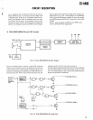
In the transmitter second mixer, consisting of Q1 1 and Q12
,
(3SK122), the 8
.83 MHz transmit IF signal input to the R
F
unit is mixed with HET oscillator signal (36
.22 MHz) fro
m
the PLL unit and converted to 45
.05 MHz signals
. The 45
.0
5
MHz signal goes through D23 and the MCF to remove an
y
spurious components
. The 45
.05 MHz signal then goe
s
through D27 and is supplied to the transmit third mixer con
-
sisting of Q13 and Q14 (3SK1 22)
. In the third mixer the sig
-
nal is mixed with VCO signal (Q21 to Q24) amplified by Q1
2
(2SC2668) and converted to the required transmit frequen
-
cy (1
.8 to 29
.7 MHz)
. The signal from the third mixer goe
s
through the low pass filters C156, C158, C159, and L89
,
and is amplified by the wide band amplifier Q15 (2SC2570)
.
The signal then goes through the wide band transformer Ti
9
and low pass filters C164, C165, and L90, and is further am
-
plified by wide band amplifier Q16 (2SC2538)
. The signa
l
from the Q16 goes through the output transformer T20 an
d
is used as the drive output
.
In FM mode, the PLL VCO is directly modulated
. The audi
o
signal from IF unit IC4 (UPC1 1 58HZ) is fed into the RF uni
t
via the FM1 pin
. In the RF unit, the audio signal is amplifie
d
by Q36 (2SC2459) and Q37 (2SC2603), and goes throug
h
the limiter circuit consisting of Q38 (UPC4558C) and lo
w
pass filter circuit, and is sent to the PLL unit via the FM
D
pin
. In the PLL unit, the 36
.22 MHz VCO is modulated
. Q3
9
(2SC2603) is a switching circuit to prevent the modulate
d
signals from being emitted from the PLL unit in a mode othe
r
than FM
.
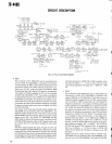
For
"S"
model radios the output from the RF unit i
s
amplified to a 100 W power level by Q1 (2SC2075), Q
2
and Q3 (2SC2509), and Q4 and Q5 (2SC2879) in th
e
final unit
. The 100 W output goes through the LPFs whic
h
differ by bands, and is sent as output to the antenna via th
e
AT unit and transmit/receive switching relay
. SWR an
d
ALC detection is performed at the output of the LPFs
.
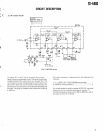
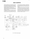
1) Antenna tune
r
The antenna tuner operates when the AUTO/THRU switc
h
is in the AUTO position and the AT TUNE switch is ON
. Th
e
antenna tuner is driven in the CW mode and power is reduce
d
to 50 W by the microcomputer regardless of the mode select
-
ed before the AT TUNE switch was turned ON
. The rang
e
of operating frequencies is determined by a microcompute
r
program, and is from 3
.5 MHz to 30 MHz
.
• AT unit operatio
n
Power transmitted by the final unit passes through the cur
-
rent and voltage detecting transformers L1 and L2 usin
g
toroidal cores
. Current and voltage components detecte
d
by the transformers are supplied to pins 9 and 13 of IC
2
for wave shaping and their phases are compared by IC
3
HD10131
. The output from pin 3 of IC3 depends upo
n
the phase of the voltage and current waveforms applie
d
to IC3
. The signal from IC3 pin 3 is sent to pins 10 an
d
15 of buffer IC IC3 HD10125
. Output from pins 12 an
d
13 of IC3 goes through level shift Zener diodes D5 an
d
D6 to control the input circuit of motor drive IC IC
5
BA6109U2
. The output signal is used to drive motor M
1
to adjust the variable capacitor VC1 so that the phas
e
difference between voltage and current components i
s
reduced
.
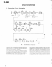
The current and voltage components output from the cur
-
rent and voltage detecting transformers is also supplie
d
to the voltage comparator IC1 NJM2903D
. The compa-
rator output is used by motor drive IC IC6 BA6109U2 t
o
drive motor M2 to adjust variable capacitor VC2 so tha
t
the amplitude difference is reduced
. That is, the phase con
-
trol variable capacitor VC1 is controlled so that the cur
-
rent is in phase with the voltage and the voltage contro
l
variable capacitor VC2 is controlled so that the amoun
t
of amplitude difference between the current and voltag
e
is reduced (SWR1, an SWR of 1 to 1, is obtained whe
n
the current and voltage are in phase and the amount o
f
amplitude difference is 0)
. VC1 and VC2 are designed t
o
operate independently of each other, but since phas
e
difference affects the amount of amplitude difference an
d
vice versa, VC 1 and VC2 will normally rotate together
.
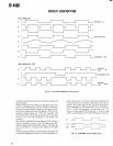
Forward and reflected waves detected by the filter unit ar
e
converted to SWR control signals in the SWR arithmetic cir-
cuit in the control unit and are sent to the ISW pin of th
e
AT unit
. Since the SWR control signals are current wave
-
forms, the signals are converted from Ito V waveforms b
y
IC8 (b/4) in the AT unit and to obtain the corresponding vol
-
tage mode SWR signals are generated
. The SWR signals ar
e
then fed into the SWR comparator IC8 (C/4)
. The referenc
e
voltage pin 9 of the IC8 (C/4) is supplied with a voltage cor
-
responding to an SWR of 1
.25 to 1 via a potentiometer
.
Therefore, when the actual SWR value exceeds 1
.25, pin
8
of SWR comparator IC8 (C/4) is H, so the motor drive vol-
tage control transistor Q5 turns on and the collector of Q
4
is supplied with voltage from pin 14S
. The voltage is als
o
used to turn the tuning LED on. The inverted input pin of IC
8
(d/4) is supplied with triangular waves generated by IC7, an
d
its non-inverted input pin is supplied with the above SWR vol
-
tage signals
. As a result, as SWR lowers, IC8 (d/4) outputs
11