


TS-440S
CIRCUIT DESCRIPTIO
N
VCO I A 45
.08
.
. 52
.55 MH
z
8 52
.55
..
. 59
.55 MH
z
C 59
.55
.
. 67
.05MH
z
D 67
.05
.,
. 75
.05MHz
Q3
6
I
fLO
J
---
-
024
2502459
.
2
034,3
5
IC
1
3
Di
v
4
9MH
z
BUF
F
2502668
SN7RS,12
N
6
r ST
D
ST
D
OSC
Q2
1
250278
7
Q2
2
BUF
F
2SC266
8
BPF
O
FM MO
D
0
9
UFF
I
I
36
.22MHZ
037
03
8
118111 FM
)
3
I C
SN 74LS9
0
IC
2
4
.55MH
z
LPF
7244 9MH
z
15KHZ1
20KHZ
: FM
I
6 14
7
IC18
250245
8
AMR,FMR
: O
N
/456
.5KHZ USB,C
W
1453
.5KHZ LSB,FSK
1
`\
AMR,FM
R
®
to
-
Q
6
AMT , FM
T
455KHZ
Q
7
25C266B
(OCT
I
4508-
.]5G5MH
=
. .
LO
256192
4
Q25
1
8 375MH
z
SN16913
8
0
.175-30
.675M
H
023
BUF
F
SNI6913F 250266
8
IC1I
IC8
6
.53-
.6
.63MHZ
10
7
2502668
VC
O
25C266B
55
A
5
vco
Co
D
ICI4
SN15913
3
5
.82
5
P
5 32 5
8
.5539
.05 MH
z
2502668
2S 0266822
020
0
AM,F
M
91MHZ /91
.3MHZ
. USB
4
O
w
2SC2668 90
.7MHZ
: LSH
.FS
K
A
.LPF
o
3l
,
32
,
33
2502459 x
3
}
500KH
z
P
.
_
PHA
. C
.
1017
9MH
x
3-]3
1
i
PLL
II
6
.5-
.36
.5MH
Q2
6
2SC2668
IC1
2
2SC245
8
BUFF
L
DIV
SN74SII2N
IC1
6
1/30,1/2
SN74SION
IC1
5
4
030
029
Q27,2
8
\
2SC2668
HET
CA
R
SFT
CA
R
05
2SC2668
2502458
250195
9
2SC266
8
15K Hz
(
P
D
111
019
5
SN16913
P
2SC2668
459
L
SN16913P 2502458
PL L
4
01,
2
25031132
2
IC1
0
54460
L
58
.25-53
.25MHz
Q1
8
016,17
I
PLL
3
2502668 2SC266
8
I20KHZI
IC9
015
01
3
2502668
®
9MHz K 1820
0
I/ 18260
: USB , C
w
\18140 LS8,FS
K
IF SHIFT I-40--40
1
CAR
I-16-
. 15
)
B
.A
P
A
LPF
h-1
P
.
D
I
'PHA
. C
.
2503113 x 2
S 1 R
MN6147 2802668
99
.
-IO
4
Q12
250266
6
IC
5
64
.78-59
.88MHz 1
.98-2
.08M4z
IC
6
/
5
01
4
BUF
F
LPF
DI
V
I/1
0
B P F
MN6147
C I
SN74LS90N M54460L
2SC266
8
M 9MHz
010,11
(5K
H
3239
.
. 2994 (STEP 51
A
. LPF
P D
_ IC
4
HA C
MN 614
7
2503113
. 2
L 9MHz
RITZ-120- ,120
1
19800- 2079
9
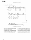
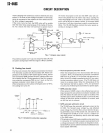
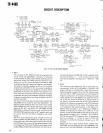
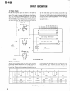
Fig
. 12
PLL circuit block diagra
m
•
PLL
4
PLL4 consists of IC1 (MN6147) and its associated loo
p
circuit
. VC04, Q3 (2SC2668), is locked at a frequenc
y
of aproximately 91 MHz, which differs depending on th
e
operational mode
. The 9 MHz reference frequency is ap-
plied to pin 3 of ICI, where the signal is divided by 180
0
to generated the 5 kHz signal for frequency comparison
.
The output of VC04 is supplied to IC1 pin 16 via buffe
r
amplifier Q4 (2SC2668)
. In ICI, the output is divided b
y
an appropriate division ratio (18200 or so) which differ
s
depending on the mode
. The phase of the signal is com-
pared with that of the 5 kHz reference signal by the phas
e
comparator and the VC04 oscillation frequency is locked
.
Frequency division data is sent from the digital unit (DA
O
to DA3 and CK3)
.
The output from PLL4 goes through buffer amplifier Q
5
(2SC2668) and is divided by 20 in IC2 (M54459L(
. Th
e
signal is further divided by ten in the carrier circuit of IC
3
(SN74LS90N) and then fed into the IF unit as the carrie
r
signal via the LPF, and buffer Q7 (2SC2458) and Q
8
(2SC 1959)
. In AM or FM receive mode, switching circui
t
Q6 (2SC2458) operates when an SFT signal is sent, an
d
as a result, IC3, Q7, and Q8 are stopped to cut carrie
r
signals
.
The PLL4 output signal also goes through the LPF an
d
buffer amplifier Q9 (2SC2458) and is fed into the mixe
r
in the main loop, where the signal is used to form the dig
-
ital VFO signal
. As a result, the operating frequency doe
s
not change even if the carrier frequency is changed, whic
h
enables USB and LSB mode switching IF shift and fine car
-
rier point adjustment
. In SSB, CW, or FSK reception mode
,
the may be shifted +/– 1 kHz or more and the carrie
r
point can be adjusted in the range from – 400 Hz to + 35
0
Hz
.
•
PLL
3
PLL3 consists of IC4 (MN6147) and its associated loo
p
components
. VCO3, Q12 (2SC2668), is locked in th
e
range of 99 MHz to 103.995 MHz
. The 9 MHz referenc
e
frequency signal is supplied to pin 3 of IC4, where the sig
-
nal is divided by 1800 to generate the 5 kHz signal fo
r
frequency comparison
. The output of VCO3 goes throug
h
buffer amplifier Q13 (2SC2668) and is applied to IC4 pi
n
16
. In IC4, the output is divided by L and the phase o
f
the signal is compared with that of the 5 kHz referenc
e
signal by the frequency comparator, and VCO3 oscillatio
n
frequency is locked (in 5 kHz steps)
. The division ratio
,
L, is supplied by the microprocessor, in the digital unit
,
(DAO to DA3 and CK2)
. L is in 1000 steps (19800 t
o
20799) corresponding to 0
.00 kHz to 9
.99 kHz
. In C
W
receive, in order to obtain 800 Hz beat signals in the oper
-
ation frequency display, the L is shifted
-80
(19720 t
o
20719) and when RIT/XIT operates, the Lis changed s
o
that fvco is shifted +1– 1
.2 kHz or more
. In AM or F
M
mode, the L is shifted by 10 steps to change
fvco
by 10
0
Hz steps
.
Output from PLL 3 goes through buffer amplifier Q1
4
(2SC2668) and it is divided by ten in IC5 (M54460L) an
d
then by five in IC6 (SN74LS90N)
. The signal is then fe
d
16