


TS-440
S
CIRCUIT DESCRIPTIO
N
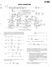
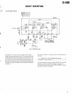
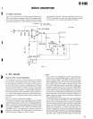
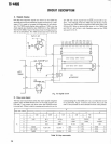
Vs
F
is compared with voltage from IC8 pin 6 (5
.5 V)
.
When SWR increases,
VSF
lowers and the voltage leve
l
of IC8 pin 8 rises
. At IC7 pin 3, a triangular wave is moni
-
tored
. The triangular wave is compared with the wav
e
from IC8 pin 8 and output
. The triangular wave is con-
verted to a square wave by IC10 and sent to switch Q
3
and Q4
. This voltage is used as the SWR control voltage
.
Output voltage from IC8 pin 2 consists of the voltage com
-
pared with VsR/Vs
F
and + 5 DC voltage
. It is distribute
d
to IC4 the level shift/meter amplifier to move the needl
e
in the SWR meter and IC5 the V-I convertor to control th
e
AT440
.
VR14 is used to adjust the SWR meter ZERO point
.
VR 13 is for SWR meter adjustmen
t
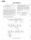
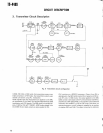
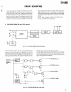
3) FULL/SEMI BREAK-IN and VOX circuits
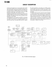
RL TXB RX
B
MICROPROCESSOR
STAND-B
Y
CIRCUIT
CONTROL
POWER SUPPL
Y
CONTRO
L
CIRCUIT
KEYIN
G
CIRCUI
T
VO
X
CIRCUIT
Fig
. 9-1 FULL/SEMI BREAK-IN block diagra
m
When the standby switch, the key, or the VOX switchin
g
transistor are activated, a ground is applied to the input pi
n
of the control circuit, which causes a standby signal to b
e
fed to the microprocessor to determine if a valid transmit con
-
dition has been met
. When that condition has been met, th
e
KEYIN
G
STAND-B
Y
VOX
standby circuit in the IF unit will be turned on
.
A keying signal is generated by the control circuit, wheneve
r
the key is depressed, to control the keying circuits in the I
F
unit
. This keying signal is also used as the transmit/receiv
e
signal during break-in operations
.
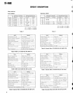
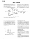
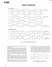
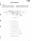
o KEYING (FULL
)
o CONTROL( FULL
)
o KEYING(SEMI
)
0
CONTROL(SEMI
)
Fig
. 9-2 FULL/SEMI BREAK-IN timing chart
13