


TS-440
S
(
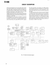
CIRCUIT DESCRIPTIO
N
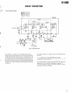
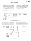
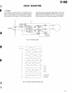
into pin 2 of MIX5 IC7 (SN1 691 3P) via the LPF
. In MIX5
,
the signal is mixed with the signal generated by PLL4 an
d
goes through the BPF to generate a signal in the range o
f
6
.53 MHz to 6
.6301 MHz (in 100 Hz steps)
. The gener-
ated signal is supplied to pin 5
.
•
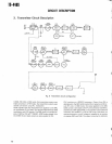
PLL
2
PLL2 consists of IC9 (MN6147) and its loop circuitry
.
VCO2, Q18 (2SC2668(, is locked in the range of 58
.2
5
MHz to 53
.2501 MHz
. The 9 MHz reference frequenc
y
signal is supplied to pin 3 of IC9, where the signal is divide
d
by 450 to generate a 20 kHz signal for frequency com-
parison
. VCO2's output goes through buffer amplifier Q1
9
(2SC2668(, and is fed into MIX4 pin 2 and mixed wit
h
the 6
.35 MHz to 6
.63 MHz signals applied to pin 5
. Th
e
mixed signal then goes through the BPF to obtain 64
.7
8
MHz to 59
.88 MHz signal (in 100 kHz steps)
. Th
e
64
.78 MHz to 59.88 MHz signal is fed into IC9_ pin 16 vi
a
buffer amplifier Q15 (2SC2668)
. In IC9, the signal is divide
d
by M, and the phase of signal is compared with that of th
e
20 kHz reference signal by the phase comparator, and thu
s
MIX4 output is locked (in 100 kHz step)
. The division ratio
M
is supplied from the digital unit (DA0 to DA3 and CK1), and i
s
in 50 steps from 3239 to 2994 corresponding t
o
0
.00 MHz to 0
.49 MHz
.
The output from PLL2 goes through buffer amplifier Q2
0
(2SC2668) and is divided by ten in IC 10 (M54460L)
. Vi
a
the LPF, the signal is fed into pin 2 of MIX3 IC1
1
(SN 16913P)
. The frequency of the signals depends on th
e
values of L and M, and is in the range of 5
.825 MHz t
o
5
.32501 MHz (10 Hz step)
.
VR1 in MIX4 circuit is used to suppress spurious output
s
from the mixer
. It is necessary to prevent PLL2 from be
-
coming unlocked
.
Signals generated by PLL2 and the 9 MHz reference fre-
quency are mixed in MIX3
. The mixed signal goes throug
h
the BPF, and is further mixed with
fLo
in MIX2 IC1
2
(SN16913P) on the IF unit
. The output from MIX2 goe
s
through the BPF to obtain 38
.55 MHz to 39.04999 MHz
.
The signals are then mixed with the output from the fina
l
VCO oscillator in MIX1
.
•
PLL
1
The last PLL loop, PLL1, consists of IC1 7 (MB87006) an
d
its loop components
. In IC 17, frequency division for refer
-
ence and comarison frequencies is set by serial data (SO
,
SCK, and LEI
. When an external prescaler is used, IC1
7
has a modulus control function for configuring the puls
e
swallow counter
.
The VCO oscillator output from the RF unit goes throug
h
Q26 (2SC2668) in the PLL unit and is fed into MIX 1
. Th
e
mixed signals go through the BPF, and they are then am
-
plified by buffer amplifiers Q27 thru Q30 (2SC2668)
,
shaped by IC 15 (SN74S 10N 1 /3), and fed into IC 1
6
(WN74S 1 12N) 1/3, or 1 /2 prescaler
. Basically, IC 16 is
a
two-level FF circuit and functions as a 1 /4 divider. But
,
when IC17 of the PLL unit sends control signals, to IC 1 6
,
IC 16 functions as a 1 /3 or 1 /2 frequency divider in con
-
junction with IC 1 5 (2/3)
. That is, the IC 1 5, IC 16, and IC1
7
form a pulse swallow frequency divider
.
The 9 MHz reference frequency signal is supplied to pi
n
1 of IC17, where the signals are divided by 18 to gener-
ate a 500 kHz signal for frequency comparison
. Signal
s
fed into IC17 pin 8 via MIX1 and the buffer amplifier ar
e
divided by N, and the phase is compared with that of th
e
500 kHz reference signals by the phase comparator
. Th
e
signal then goes through the active LPFs Q31 to Q3
3
(2SC2459) and is fed into the RF unit as VCO voltage sig
-
nals to control the variable capacitor of the final VCO
. Th
e
frequency divider N covers the full range of operating fre
-
quencies from 30 kHz to 30 MHz (500 kHz step), and i
t
has 61 steps of frequency division data supplied by th
e
microprocessor in the digital unit
.
The last VCO signal in PLL1 therefore depends on th
e
values of L, M, and N, and it is in the range from 45
.0
8
MHz to 75
.05 MHz (10 Hz step)
. N is expressed a
s
follows
:
N=PNo -
A
(No>A
)
P
:
Prescaler module valu
e
No
: Programmable counter valu
e
A
: Swallow counter valu
e
PLL IC contains No and A
.
The last VCO unit is contained in the RF unit and consist
s
of four VCOs, each handling one portion of frequencie
s
from 30 kHz to 30 MHz
. The appropriate VCO is selecte
d
by the microprocessor according to band information fro
m
the digital unit
.
•
Unloc
k
If a PLL loop enters a unlock state, the output on the U
L
pin becomes L
. This L signal is sent to the digital unit t
o
stop the microprocessor
.
•
500
kHz marker signa
l
The 500 kHz reference signal for frequency compariso
n
is supplied from IC17 pin 13, and it is used as the marke
r
reference signal
.
5
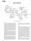
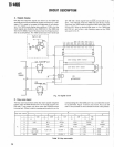
. Digital control circui
t
The TS-440 digital control circuit uses an 8-bit CPU (7800
)
which does not contain ROM, and has a 16K ROM (27128
)
and a 2K RAM 18418) outside the CPU
. A common bus use
d
for data exchange between the CPU and RAM, and betwee
n
the CPU and ROM and is also connected in parallel to th
e
two 8255's for extended I/O and an 8251 for interface t
o
a personal computer (option)
. To transfer
data
to
or
from a
n
appropriate IC, the CPU uses the WR or RD signal
,
and the chip select signal from the 74LS138
.
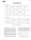
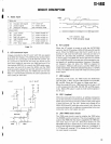
The display is dynamically controlled by software, and con-
sists of 13 digits and nine segments
. The 13 digit and seve
n
segment signal is driven by the high voltage resistive buffe
r
(6300), and the other two segment signals are driven by
a
transistor
. The 7800 transfers data serially
. The clock signa
l
is frequency divided by two in the 4013 and sent to the 6300
.
Using the 4011 and 4030, the encoder generates count
17