


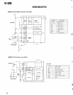
TS-440
S
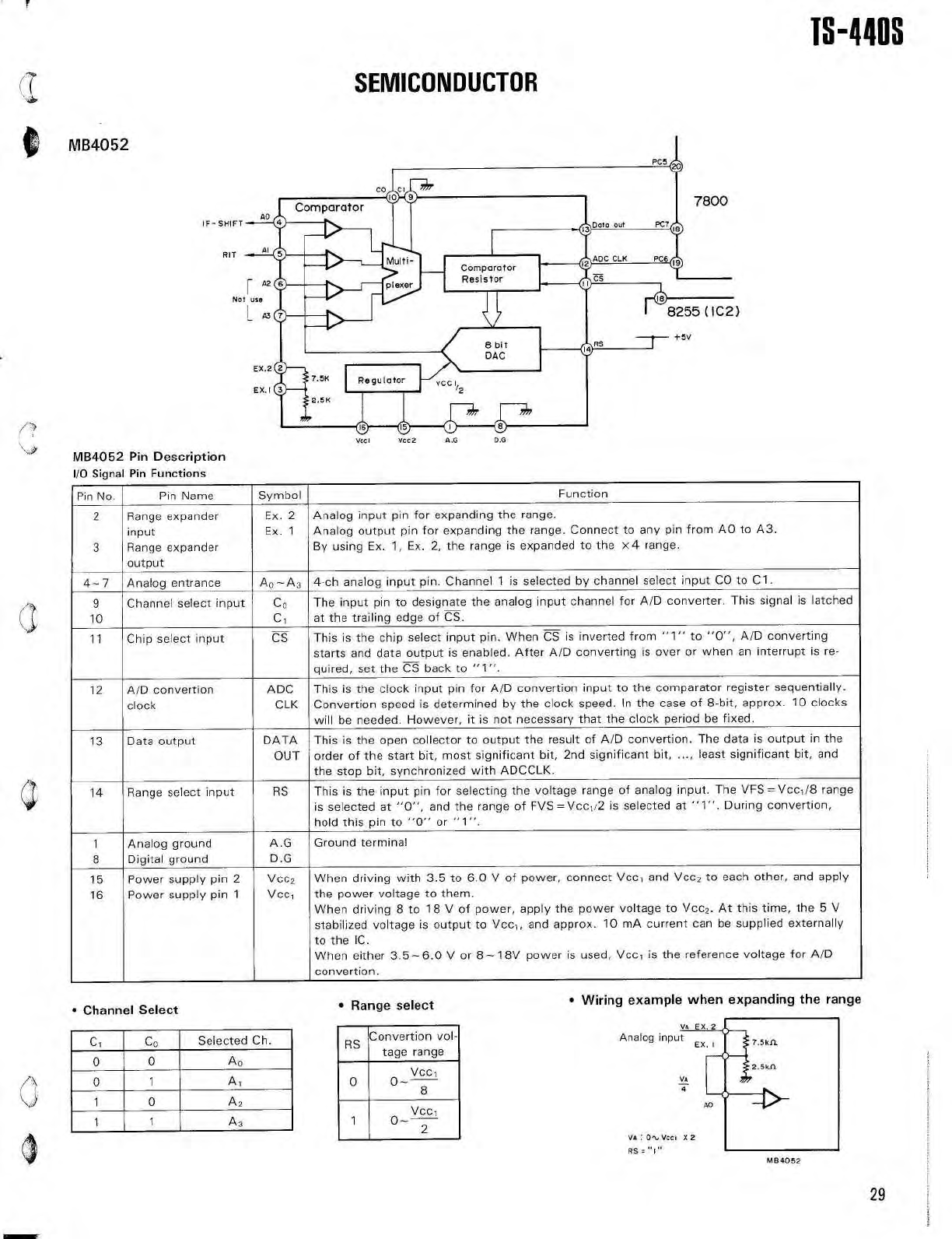
SEMICONDUCTO
R
e
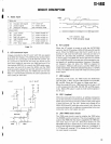
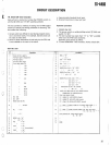
MB4052
PC
5
Co CI
7~J7
Comparato
r
Resisto
r
IF-SHIFT
-
R
Comparato
r
®
D
R IT -
AI
O
Lam,
~
,
Multi
_
D
I
ple
780
0
PC
7
12
ADC CLK
PC
6
le
8255(IC2
)
RS
+5
v
r
Ag
o
Not us
e
L
A
3
EX
.
2
EX
.!
8
bi
t
DA
C
v
CC
I
Regulato
r
2
.5
K
6
S
O
VccI
Vcc2
A
.G
D
.
G
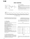
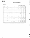
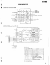
MB4052 Pin Descriptio
n
I/O Signal
Pin Function
s
Pin No
.
Pin Name
Symbol
Functio
n
2
3
Range expande
r
inpu
t
Range expande
r
output
Ex
.
2
Ex
.
1
Analog input pin for expanding the range
.
Analog output pin for expanding the range
. Connect to any pin from AO to A3
.
By using Ex
. 1, Ex
. 2, the range is expanded to the x4 range
.
4—7
Analog entrance
Ao—A
3
4-ch analog input pin
. Channel 1 is selected by channel select input CO to
Cl
.
9
10
Channel select input
C
o
C,
The input pin to designate the analog input channel for A/D converter
. This signal is latche
d
at the trailing edge of CS
.
11
Chip select input
CS
This is the chip select input pin
. When CS is inverted from
"1"
to "0", A/D convertin
g
starts and data output is enabled
. After A/D converting is over or when an interrupt is re
-
quired, set the CS back to "1"
.
12
A/D convertio
n
clock
AD
C
CLK
This is the clock input pin for A/D convertion input to the comparator register sequentially
.
Convertion speed is determined by the clock speed
. In the case of 8-bit, approx
. 10 clock
s
will be needed
. However, it is not necessary that the clock period be fixed
.
13
Data output
DAT
A
OUT
This is the open collector to output the result of A/D convertion
. The data is output in th
e
order of the start bit, most significant bit, 2nd significant bit,
. .
., least significant bit, an
d
the stop bit, synchronized with ADCCLK
.
14
Range select input
RS
This is the input pin for selecting the voltage range of analog input
. The VFS=Vcc,/8 rang
e
is selected at "0", and the range of FVS=Vcc,i2 is selected at "1"
. During convertion
,
hold this pin to
"0"
or "1"
.
1
8
Analog groun
d
Digital ground
A
.
G
D
.G
Ground termina
l
1
5
16
Power supply pin
2
Power supply pin 1
Vcc
2
Vcc
1
When driving with 3
.5 to 6
.0 V of power, connect Vcc, and Vcc
2
to each other, and appl
y
the power voltage to them
.
When driving 8 to 18 V of power, apply the power voltage to Vcc
2
. At this time, the 5
V
stabilized voltage is output to Vcc,, and approx
. 10 mA current can be supplied externall
y
to the IC
.
When either 3
.5--6
.0 V or 8— 18V power is used, Vcc, is the reference voltage for A/
D
convertion
.
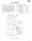
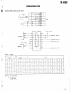
•
Channel Select
•
Range select
• Wiring example when expanding the rang
e
RS
'Convertion
vol
-
tage rang
e
Vcc
,
0
0—'
8
Vcc
,
1
0--'
2
C
,
0
C
o
0
Selected Ch
.
A
o
1
A
,
0
1
0
1
1
A
2
A
3
MB4052
2
9