


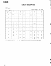
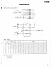
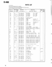

TS-440S
SEMICONDUCTO
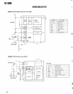
R
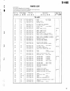
APD63000 (Display unit IC1
)
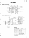
Pin description
Pin No
.
Symbol
Pin name
I/O
Descriptio
n
1
01
3
014
FI
P
015
Segmen
t
driver
0
High dielectric-strength (40V) output in the Pch open
.
017
(
0
13'
019)
Corresponds to the output of
Q13
—
Q1
9
01
8
7
01
9
8
SO
Serial data output pin
0
Output serial data the trailing edge of SCK
. When the n-numbe
r
of
pPD63000s
are connected in series, this can be connected t
o
the SI of the following stage
.
9
BI
Blanking pin
This input can turn off all indicator or displays, and can dim the
m
by applying a random duty pulse from outside
. Active low
.
10
LH
Latch pin
I
Transmits the connects of the serial shift register to the buffe
r
register at low level, to latch the connects at the rising time
.
Active rising (leading) edge
.
11 SI
Serial data input pin
I
This is the data input pin
. Inputs data to the shift register at th
e
rising edge of SCK
.
Reads out the SI data to the shift register at the rising edge o
f
12
SCK
Serial clock input pin
I
SCK
.
Outputs data from SO at the trailing edge of SCK
.
13
CS Chip select pin
When CS is high, this inhibits SCK and LH, and when CS is low
,
activates SCK and LH
.
14
Vss
GND
Connect to the GND terminal of the system
.
15
0
0
16
0
1
Pch open-drain system, high dielectric-strength output
.
17
0
2
18
0
3
FIP
Corresponds to th
e
0
4
output of 0o to
012
V0
0
0
5
Segmen
t
Qg
driver
Pc
h
07
r
1
p
0
8
O
9
(00
—
012)
0
26
Ot
o
0
11
Vss
Oo
Ot
s
27
01
2
28
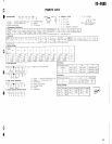
V00
Power supply pin
—
5 V ± 10%
)
)
34