


2004 Jan 26 67
Philips Semiconductors Product specification
MPEG-2 video and MPEG-audio/AC-3
audio encoder with multiplexer
SAA6752HS
14 SOLDERING
14.1 Introduction to soldering surface mount
packages
This text gives a very brief insight to a complex technology.
A more in-depth account of soldering ICs can be found in
our
“Data Handbook IC26; Integrated Circuit Packages”
(document order number 9398 652 90011).
There is no soldering method that is ideal for all surface
mount IC packages. Wave soldering can still be used for
certain surface mount ICs, but it is not suitable for fine pitch
SMDs. In these situations reflow soldering is
recommended.
14.2 Reflow soldering
Reflow soldering requires solder paste (a suspension of
fine solder particles, flux and binding agent) to be applied
to the printed-circuit board by screen printing, stencilling or
pressure-syringe dispensing before package placement.
Driven by legislation and environmental forces the
worldwide use of lead-free solder pastes is increasing.
Several methods exist for reflowing; for example,
convection or convection/infrared heating in a conveyor
type oven. Throughput times (preheating, soldering and
cooling) vary between 100 and 200 seconds depending
on heating method.
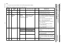
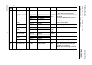
Typical reflow peak temperatures range from
215 to 270 °C depending on solder paste material. The
top-surface temperature of the packages should
preferably be kept:
• below 225 °C (SnPb process) or below 245 °C (Pb-free
process)
– for all BGA, HTSSON-T and SSOP-T packages
– for packages with a thickness ≥ 2.5 mm
– for packages with a thickness < 2.5 mm and a
volume ≥ 350 mm
3
so called thick/large packages.
• below 240 °C (SnPb process) or below 260 °C (Pb-free
process) for packages with a thickness < 2.5 mm and a
volume < 350 mm
3
so called small/thin packages.
Moisture sensitivity precautions, as indicated on packing,
must be respected at all times.
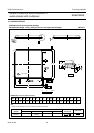
14.3 Wave soldering
Conventional single wave soldering is not recommended
for surface mount devices (SMDs) or printed-circuit boards
with a high component density, as solder bridging and
non-wetting can present major problems.
To overcome these problems the double-wave soldering
method was specifically developed.
If wave soldering is used the following conditions must be
observed for optimal results:
• Use a double-wave soldering method comprising a
turbulent wave with high upward pressure followed by a
smooth laminar wave.
• For packages with leads on two sides and a pitch (e):
– larger than or equal to 1.27 mm, the footprint
longitudinal axis is preferred to be parallel to the
transport direction of the printed-circuit board;
– smaller than 1.27 mm, the footprint longitudinal axis
must be parallel to the transport direction of the
printed-circuit board.
The footprint must incorporate solder thieves at the
downstream end.
• For packages with leads on four sides, the footprint must
be placed at a 45° angle to the transport direction of the
printed-circuit board. The footprint must incorporate
solder thieves downstream and at the side corners.
During placement and before soldering, the package must
be fixed with a droplet of adhesive. The adhesive can be
applied by screen printing, pin transfer or syringe
dispensing. The package can be soldered after the
adhesive is cured.
Typical dwell time of the leads in the wave ranges from
3 to 4 seconds at 250 °C or 265 °C, depending on solder
material applied, SnPb or Pb-free respectively.
A mildly-activated flux will eliminate the need for removal
of corrosive residues in most applications.
14.4 Manual soldering
Fix the component by first soldering two
diagonally-opposite end leads. Use a low voltage (24 V or
less) soldering iron applied to the flat part of the lead.
Contact time must be limited to 10 seconds at up to
300 °C.
When using a dedicated tool, all other leads can be
soldered in one operation within 2 to 5 seconds between
270 and 320 °C.