


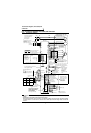
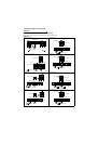
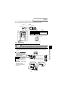
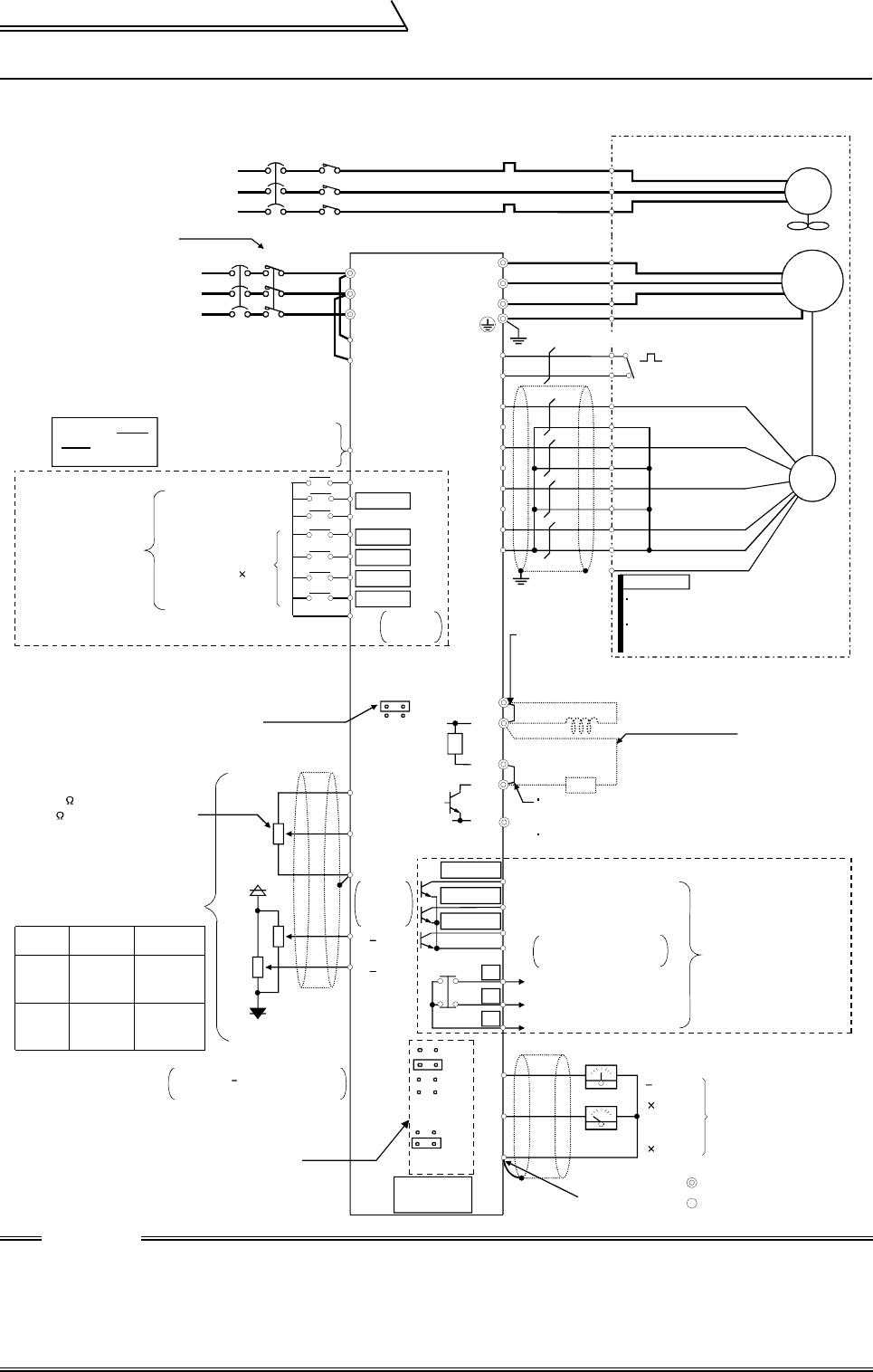
7
Connection diagram, PLG cable, PU
connector
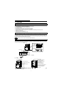
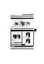
2.2 Connection diagram, PLG cable, PU connector
2.2.1 Connection diagram
CAUTION
• To prevent a malfunction caused by noise, separate the signal cables more than 10cm from the power
cables.
• During wiring, do not leave wire off-cuts in the inverter.
Wire off-cuts will cause an alarm, failure or malfunction. Always keep the inverter clean. When drilling
mounting holes in a control box etc., take care not to allow chips and other foreign matter to enter the
inverter.
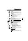
3-phase AC
power supply
Take care not to
short terminals
PC-SD.
Avoid frequent ON-OFF.
Repeated inrush currents at
power-on will shorten the
converter life.
(Switching life is 100,000)
NFB MC
External transistor common
24VDC power supply
Contact input common (source)
Terminals DI1 to
DI4 and STR vary
in function with
the input terminal
function selection
(Pr. 180 to Pr. 183,
Pr. 187) settings.
Forward rotation start
Reverse rotation start
Reset
Control input signals (no voltage input allowed)
Digital input
signal 4
STF
STR
RES
DI1(RL)
DI2(RM)
DI3(RH)
DI4(RT)
SD
Match phase sequence.
Jumper
(When using the
FR-BEL, remove
this jumper.)
Contact
input
common
Earthing (Grounding)
FR-BEL power factor
improving DC reactor
(option)
FR-ABR high-duty
brake resistor
(option)
Jumper (Remove this jumper
when using the FR-ABR.)
Terminal PX is provided for
the 5.5K or less.
Across terminals P
and PR, connect only
the optional,
recommended brake
resistor. In addition,
never short these
terminals.
Terminal PR is
provided for the 15K
or less.
(Open collector output)
Open collector output
common
Terminals DO1 to DO3
and ABC vary in function
with the output terminal
function selection
(Pr. 190 to Pr. 192,
Pr. 195) settings.
Meter
12 bits
12 bits
Monitor output
(Analog output common)
Main circuit terminal
Control circuit terminal
Any of three different
signals can be selected
using the parameter.
10V
1ch
+
0 to 10V
1ch
R
S
T
R1
S1
PC
V
W
OH
SD
PA
PAR
PB
PBR
PZ
PZR
P1
P
PX
PR
R
N
SE
DA1
DA2
5
U
V
W
U
E
PLG
R
IM
(-)
(+)
C
B
A
(RUN)
DO1
DO2
DO3
(SU)
(IPF)
REMARKS
5V
12V
24V
EXT
Differential
Complimen-
tary
Alarm output
(Contact output)
PG
SD
SINK
SOURCE
load impedance of 10kW or more
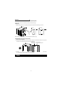
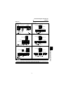
Vector inverter
(FR-V500)
Analog command
input
Terminal
Speed setting potentiometer
1/2W 1k
2W 1k is recommended for use
when speed setting is changed
frequently.
External
power supply
Prepare a 10V external power
supply for terminals 1, 3.
Change the jumper connector and
parameter settings according to
the PLG specifications.
Analog
input
common
Torque
Control
Speed
Control
Speed
restriction
command
Torque
command
Torque
restriction
command
Main
speed
command
+
1( 10V)
3( 10V)
+
+
10E, 2, 5
3
2
10E
(+10V)
+10V
1
2
3
5
-10V
(0 to +10V)
PU
connector
You can select between sink and source
(class D earthing (grounding))
(Dedicated Motor: SF-V5R)
When the motor used is not the vector
inverter motor, the pin numbers are different.
The N pin of the PLG designed for vector
inverter motor is case-earthed.
A
B
C
D
G
S
R
F
N
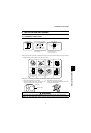
NFB MC
Match phase sequence.
(Fan should have intake rotation.)
R
S
T
FAN
OCR
A
B
C
Verify the power specification
of the motor cooling when
performing wiring.
Thermal
protector
When using the motor
not equipped with a
thermal protector,
set Pr. 9 and Pr. 876
= "0"
G1
G2
Change the jumper connector and
parameter settings according to
the PLG specifications.
Refer to page 12 for details.
Refer to page 16 for details.
Refer to page 99