


SE7501WV2 Connectors Intel® Server Board SE7501WV2 TPS
Revision 1.0
Intel reference number C25653-001
154
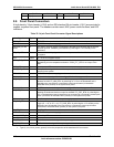
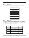
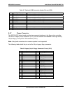
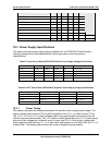
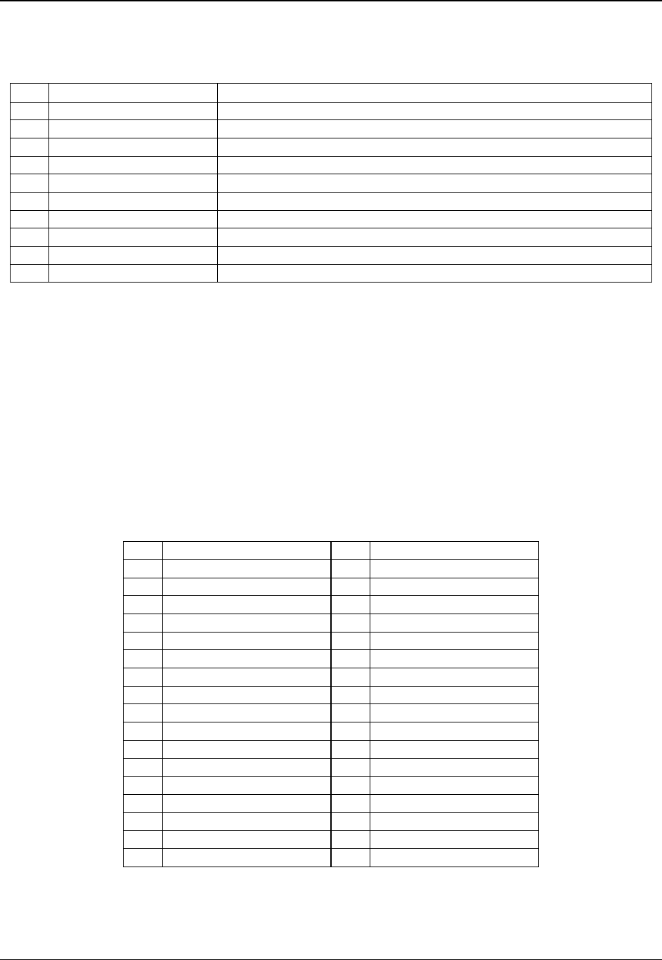
Table 87. Optional USB Connection Header Pin-out (J1D3)
Pin Signal Name Description
1 VREG_FP_USBPWR0 Front Panel USB Power (Ports 0,1)
2 VREG_FP_USBPWR0 Front Panel USB Power (Ports 0,1)
3 USB_FP_P0- Front Panel USB Port 0 Negative Signal
4 USB_FP_P1- Front Panel USB Port 1 Negative Signal
5 USB_FP_P0+ Front Panel USB Port 0 Positive Signal
6 USB_FP_P1+ Front Panel USB Port 1 Positive Signal
7 Ground
8 Ground
9 Key
10 USB_FP_OC0 Front Panel USB Overcurrent signal (Ports 0,1). This signal is not used
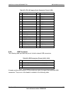
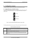
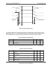
8.6.7 Floppy Connector
The SE7501WV2 server board provides two separate interfaces to the floppy drive controller.
The first is a legacy 34-pin connector (J1G1), and the second is embedded in the high-density
100-pin floppy / front panel / IDE connector (J2G1).
Note: Using both connectors in a common system is not supported.
The following tables detail the pin-out of the 34-pin legacy floppy connector.
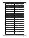
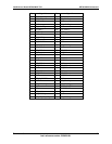
Table 88. Legacy 34-pin Floppy Connector Pin-out (J1G1)
Pin Signal Name Pin Signal Name
1 GND 2 FD_DENSEL0
3 GND 4 Test Point
5 KEY 6 FD_DENSEL1
7 GND 8 FD_INDEX_L
9 GND 10 FD_MTR0_L
11 GND 12 FD_DS1_L
13 GND 14 FD_DS0_L
15 GND 16 FD_MTR1_L
17 Test Point 18 FD_DIR_L
19 GND 20 FD_STEP_L
21 GND 22 FD_WDATA_L
23 GND 24 FD_WGATE_L
25 GND 26 FD_TRK0_L
27 Test Point 28 VCC
29 GND 30 FD_RDATA_L
31 GND 32 FD_HDSEL_L
33 GND 34 FD_DSKCHG_L