


Intel® Server Board SE7501WV2 TPS Functional Architecture
Revision 1.0
Intel reference number C25653-001
37
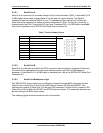
For example, Modem applications typically use a DCD signal. In this case the user would use a
DCD-configured adapter and set the jumper block as shown in Figure 5.
3.3.2.4 Floppy Disk Controller
The floppy disk controller (FDC) in the SIO is functionally compatible with floppy disk controllers
in the DP8473 and N844077. All FDC functions are integrated into the SIO including analog
data separator and 16-byte FIFO. The SE7501WV2 server board provides two separate
interfaces for the floppy disk controller. The first is a SSI compliant 36-pin connector, and the
second is through the high-density 100-pin floppy / front panel / IDE connector.
Note: Using both interfaces in a common configuration is not supported.
3.3.2.5 Keyboard and Mouse
One external PS/2 port located on the back of the baseboard is provided for either a keyboard
or a mouse. A PS/2 Y-cable can be used to provide simultaneous support for both a keyboard
and mouse.
3.3.2.6 Wake-up Control
The Super I/O contains functionality that allows various events to control the power-on and
power-off the system.
3.3.3 BIOS Flash
The SE7501WV2 server board incorporates an Intel
®
3 Volt Advanced+ Boot Block 28F320C3
Flash memory component. The 28F320C3 is a high-performance 32-megabit memory
component that provides 2048K x 16 of BIOS and non-volatile storage space. The flash device
is connected through the X-bus from the SIO.