


Intel® Server Board SE7501WV2 TPS Functional Architecture
Revision 1.0
Intel reference number C25653-001
25
populated in order for the system to boot. If additional banks have less than two DIMMs, the
memory for that bank(s) will not be available to the system.
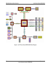
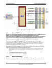
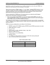
There are three banks of DIMMs, labeled 1, 2, and 3. Bank 1 contains DIMM locations 1A and
1B, Bank 2 contains 2A and 2B, and Bank 3 contains 3A and 3B. DIMM socket identifiers are
marked with silkscreen next to each DIMM socket on the baseboard. Note that the sockets
associated with any given bank are located next to each other.
Certain combinations of DIMM types in the same system can violate the write Ringback
measurement specification during analog validation.
• When mixing double-ranked DIMMs (x4 or x8) with single-ranked DIMMs (x4 or x8), if a
single-ranked DIMM is placed in the populated slot closest to the MCH, the Write Ringback
at that DIMM violates the JEDEC DRAM specification.
The baseboard’s signal integrity and cooling are optimized when memory banks are populated
in order. Therefore, when installing memory, DIMMs should be installed starting with Bank 1 and
ending with Bank 3.
DIMM and memory configurations must adhere to the following:
• DDR266 registered ECC DIMM modules (DDR200 when 400MHz processors are used)
• DIMM organization: x72 ECC
• Pin count: 184
• DIMM capacity: 128 MB, 256 MB, 512 MB, 1 GB, 2 GB
• Serial PD: JEDEC Rev 2.0
• Voltage options: 2.5 V (VDD/VDDQ)
• Interface: SSTL2
• Two DIMMs must be populated in a bank for a x144 wide memory data path.
• Any or all memory banks may be populated.
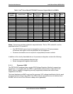
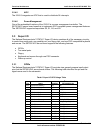
Table 3. Memory Bank Labels
Memory DIMM Bank
J5F1 (DIMM 1B), J5F2 (DIMM 1A) 1
J5F3 (DIMM 2B), J6F1 (DIMM 2A) 2
J6F2 (DIMM 3B), J6F3 (DIMM 3A) 3