


Intel® Server Board SE7501WV2 TPS Functional Architecture
Revision 1.0
Intel reference number C25653-001
27
double-bit error is detected during POST, the BIOS sends a Set DIMM State command to the
BMC indicating that the DIMM LED is lit.
3.1.2.5 Intel® Single Device Data Correction feature
The SE7501WV2 server board supports Intel’s Single Device Data Correction correct memory
architecture, which gives the memory sub-system the ability to withstand a multi-bit failure within
a DRAM device, including a failure that causes incorrect data on all data bits of the device.
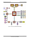
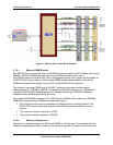
3.2 Intel
®
E7501 Chipset
The SE7501WV2 server board is designed around the Intel
®
E7501 chipset. The chipset
provides an integrated I/O bridge and memory controller, and a flexible I/O subsystem core
(PCI-X). This is targeted for multiprocessor systems and standard high-volume servers. The
Intel E7501 chipset consists of three components:
• MCH: Memory Controller Hub North Bridge. The MCH North Bridge accepts access
requests from the host (processor) bus and directs those accesses to memory or to one
of the PCI buses. The MCH monitors the host bus, examining addresses for each
request. Accesses may be directed to a memory request queue for subsequent
forwarding to the memory subsystem, or to an outbound request queue for subsequent
forwarding to one of the PCI buses. The MCH also accepts inbound requests from the
P64H2 and the ICH3-S. The MCH is responsible for generating the appropriate controls
to control data transfer to and from memory.
• P64H2: PCI-X 64bit Hub 2.0 I/O Bridge. The P64H2 provides the interface for two 64-
bit, 133MHz Rev. 1.0 compliant PCI-X buses. The P64H2 is both master and target on
both PCI-X buses.
• ICH3-S: South Bridge. The ICH3-S controller has several components. It provides the
interface for a 32-bit, 33-MHz Rev. 2.2-compliant PCI bus. The ICH3-S can be both a
master and a target on that PCI bus. The ICH3-S also includes a USB controller and an
IDE controller. The ICH3-S is also responsible for much of the power management
functions, with ACPI control registers built in. The ICH3-S also provides a number of
GPIO pins and has the LPC bus to support low speed legacy I/O.
The MCH, P64H2, and ICH3-S chips provide the pathway between processor and I/O systems.
The MCH is responsible for accepting access requests from the host (processor) bus, and
directing all I/O accesses to one of the PCI buses or legacy I/O locations. If the cycle is directed
to one of the 64-bit PCI segments, the MCH communicates with the P64H2 through a private
interface called the HI (Hub Interface). If the cycle is directed to the ICH3-S, the cycle is output
on the MCH’s 8bit HI 1.5 bus. The P64H2 translates the HI 2.0 bus operation to a 64-bit PCI-X
Rev. 1.0-compliant signaling environment operating from 100MHz to 133 MHz. The ICH3-S
translates the HI 1.5 bus operation to a 32-bit PCI Rev. 2.2-compliant signaling environment
operating at 33MHz.
The HI 2.0 bus is 16 bits wide and operates at 66 MHz with 512MT/s, providing over 1 GB per
second of bandwidth.
All I/O for the SE7501WV2 server board, including PCI and PC-compatible I/O, is directed
through the MCH and then through either the P64H2 or the ICH3-S provided PCI buses.