


Intel® Server Board SE7501WV2 TPS Configuration and Initialization
Revision 1.0
Intel reference number C25653-001
49
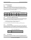
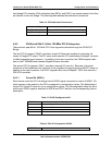
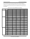
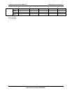
Table 17. Video Modes
Intel
®
Server Board SE7501WV2 2D Video Mode Support 2D Mode Refresh Rate (Hz)
8 bpp 16 bpp 24 bpp 32 bpp
640x480 60, 72, 75, 90, 100 Supported Supported Supported Supported
800x600 60, 70, 75, 90, 100 Supported Supported Supported Supported
1024x768 60, 72, 75, 90, 100 Supported Supported Supported Supported
1280x1024 43, 60 Supported Supported Supported Supported
1280x1024 70, 72 Supported – Supported Supported
1600x1200 60, 66 Supported Supported Supported Supported
1600x1200 76, 85 Supported Supported Supported –
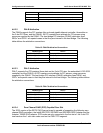
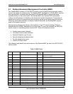
3D Mode Refresh Rate (Hz) Intel
®
Server Board SE7501WV2 3D Video Mode Support with Z Buffer
Enabled
640x480 60,72,75,90,100 Supported Supported Supported Supported
800x600 60,70,75,90,100 Supported Supported Supported Supported
1024x768 60,72,75,90,100 Supported Supported Supported Supported
1280x1024 43,60,70,72 Supported Supported – –
1600x1200 60,66,76,85 Supported – – –
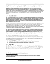
3D Mode Refresh Rate (Hz) Intel
®
Server Board SE7501WV2 3D Video Mode Support with Z Buffer
Disabled
640x480 60,72,75,90,100 Supported Supported Supported Supported
800x600 60,70,75,90,100 Supported Supported Supported Supported
1024x768 60,72,75,90,100 Supported Supported Supported Supported
1280x1024 43,60,70,72 Supported Supported Supported –
1600x1200 60,66,76,85 Supported Supported – –
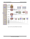
4.9.2 Video Memory Interface
The memory controller subsystem of the Rage XL arbitrates requests from direct memory
interface, the VGA graphics controller, the drawing coprocessor, the display controller, the video
scalar, and the hardware cursor. Requests are serviced in a manner that ensures display
integrity and maximum CPU/coprocessor drawing performance.
The SE7501WV2 server board supports an 8MB (512Kx32bitx4 Banks) SDRAM device for
video memory. The following table shows the video memory interface signals.
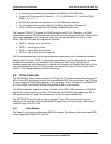
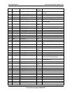
Table 18. Video Memory Interface
Signal Name I/O Type Description
CAS# O Column Address Select
CKE O Clock Enable for Memory
CS#[1..0] O Chip Select for Memory
DQM[7..0] O Memory Data Byte Mask
DSF O Memory Special Function Enable
HCLK O Memory Clock
[11..0] O Memory Address Bus