


Intel® Server Board SE7501WV2 TPS Functional Architecture
Revision 1.0
Intel reference number C25653-001
23
3.1.1.2 Reset Configuration Logic
The BIOS determines the processor stepping, cache size, etc through the CPUID instruction.
The requirements are that all processors in the system must operate at the same frequency,
have the same cache sizes, and have the same VID. No mixing of product families is supported.
On the SE7501WV2 platform, the BIOS is responsible for configuring the processor speeds.
The processor information is read at every system power-on. The speed is set to correspond to
the speed of the slowest processor installed.
Note: No manual processor speed setting options exist either in the form of a BIOS setup option
or jumpers when using production level processors.
3.1.1.3 Processor Module Presence Detection
Logic is provided on the baseboard to detect the presence and identity of installed processors.
The BMC checks the logic and will not turn on the system DC power unless the VIDs of both
processors match in a dual processor configuration.
3.1.1.4 Interrupts and APIC
Interrupt generation and notification to the processors is done by the APICs in the ICH3 and the
P64H2 using messages on the front side bus.
3.1.1.5 Server Management Registers and Sensors
The Baseboard Management Controller manages registers and sensors associated with the
processor / memory subsystem. For more information, refer to Section 5.
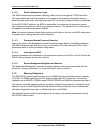
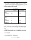
3.1.2 Memory Subsystem
The SE7501WV2 server board supports up to six DIMM slots for a maximum memory capacity
of 12 GB. The DIMM organization is x72, which includes eight ECC check bits. The memory
interface runs at 266MHz. (200MHz when DDR200 DRAM’s and 400MHz processors are used.)
The memory controller supports memory scrubbing, single-bit error correction, multiple-bit error
detection, and the Intel® Single Device Data Correction feature. Memory can be implemented
with either single sided (one row) or double-sided (two row) DIMMs.
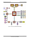
The following figure provides a block diagram of the memory sub-system implemented on the
SE7501WV2 server board.