


November 2003 © TOSHIBA TEC 7 - 1 e-STUDIO3511/4511 POWER SUPPLY UNIT
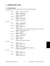
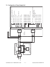
7. POWER SUPPLY UNIT
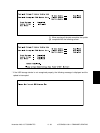
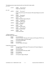
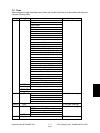
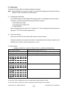
7.1 Output Channel
The followings are four output channels which are not linked with the door switch.
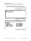
(1) +3.3V
+3.3VA : CN464 Pins 13, 14, 15 and 16
Output to the SYS board
+3.3VB : CN464 Pins 19 and 20
Output to the SYS board
+3.3VB : CN466 Pin 3
Output to the LGC board
+3.3VB : CN467 Pins 17 and 18
Output to the SLG board
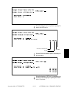
(2) +5.1V
+5.1VA : CN464 Pins 24 and 26
Output to the SYS board
+5.1VB : CN464 Pin 25
Output to the SYS board
+5.1VB : CN466 Pin 1
Output to the LGC board, CCL board (via LGC board), PFP/LCF (via LGC
board), Bridge unit (via LGC board)
+5.1VB : CN467 Pins 5 and 6
Output to the RADF
+5.1VB : CN467 Pins 21 and 22
Output to the SLG board
+5.1VB : CN468 Pin 1
Output to the finisher
+5.1VB : CN469 Pin 5
Output to the FIL board or FUS board
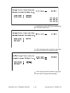
(3) +12V
+12VA : CN464 Pin 7
Output to the SYS board
+12VB : CN464 Pin 5
Output to the SYS board
+12VB : CN466 Pin 16 (*NAD/SAD/TWD models only)
Output to the LGC board
(4) -12V
-12VA : CN464 Pin 9
Output to the SYS board
-12VB : CN464 Pin 3
Output to the SYS board