


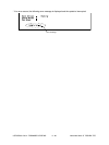
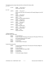
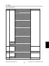
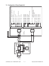
e-STUDIO3511/4511 POWER SUPPLY UNIT 7 - 2 November 2003 © TOSHIBA TEC
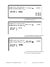
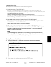
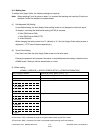
The followings are two output channels which are linked with the door switch.
(1) +5.1V
+5.1VD : CN466 Pins 11 and 12
Output to the LGC board
(2) +24V
+24VD1 : CN465 Pins 1 and 2
Output to the LGC board, CCL board (via LGC board), Bridge unit (via LGC
board)
+24VD1 : CN469 Pins 1 and 2
Output to the PFP/LCF
+24VD1 : CN470 Pin 1
Output to the power supply cooling fan
+24VD2 : CN465 Pins 5 and 6
Output to the DRV board
+24VD3 : CN467 Pins 1 and 2
Output to the RADF
+24VD4 : CN467 Pin 9
Output to the SDV board
+24VD4 : CN467 Pins 11 and 13
Output to the SLG board
+24VD5 : CN468 Pin 3
Output to the finisher
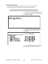
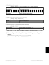
<<Output connector>>
Not linked with the door switch
CN464 For the SYS board
CN466 For the LGC board, FAX board, CCL board (via LGC board), PFP/LCF (via
LGC board), Bridge unit (via LGC board)
CN467 For the SLG board, RADF
CN468 For the finisher
CN469 For the FIL board / FUS board
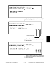
Linked with the door switch
CN465 For the LGC board, DRV board, CCL board (via LGC board), Bridge unit
(via LGC board)
CN466 For the LGC board
CN467 For the SLG board, SDV board, RADF
CN468 For the finisher
CN469 For the PFP/LCF
CN470 For the power supply cooling fan