


CSA 803C Service Manual
3Ć7
Block Diagram Descriptions
This section describes the CSA 803C detailed block (cabling) diagram and
the boardĆlevel block diagrams (see the Diagrams section).
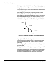
The A1 M/F Strobe Drive board consists of the following circuits:
H Data buffers circuitry
H Address latch circuitry
H Function decoder circuitry
H Internal clock rate generator circuitry
H Control buffers circuitry
See Figure 9Ć2 for a block diagram of this board.
Data Buffers
This circuit buffers the A5 Time Base/Controller board's address and data
buses with bidirectional buffers, and the A5 Time Base/Controller board's
control lines with octal buffers.
Address Latch
This circuit buffers and latches the address for the A5 Time Base/Controller
board to use.
Function Decoder
This circuit partially decodes this latched address and enables the data
buffers if the address is on this board or the A27 & A28 Acquisition system
boards (controlled through this board). The function decoder also selects
the appropriate direction of the data buffers to perform a read or write operaĆ
tion.
Internal Clock Rate Generator
This circuit is a 16Ćbit programmable counter that is tied to the ÷ 2 flipĆflop
that produces the square wave output. The overall division ratio of this block
can be programmed from 2
2
to 2
17
. The internal clock rate generator is
programmed at powerĆon to provide a 100 kHz output given a 4 MHz input
on jumper J35.
A1 M/F Strobe Drive
Board