


Block Diagram Descriptions
Theory of Operation
3Ć18
The A13 Mother board provides the interconnection for the microprocessor
signals and the +5 V power among the following boards:
H A14 I/O board
H A15 Memory Management Unit (MMU) board
H A17 Executive Processor board
H A18 Memory board
The A14 I/O board contains the following circuitry:
H Data buffers
H Timer configuration circuitry
H Real time clock
H Serial data interface (SDI)
H Temp/tone readback buffer
H Tone generator
H GPIB control circuitry
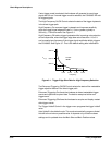
See Figure 9Ć8 for a block diagram of this board.
The A14 I/O board is an interface between the Executive Processor (EXP)
and devices on the A9, A10, and A11 Front Panel boards, the A12 Rear
Panel assembly, and onĆboard I/O devices. The EXP reads and writes to
these I/O devices at specific I/O addresses. These I/O addresses are deĆ
coded to produce device select signals which enable the addressed device.
Each I/O device is located on I/O address boundaries of at least 100
hex
.
The lower eight bits of the Executive data bus transmit data to and from the
various I/O devices. Note that only one I/O device can be accessed at a
time.
I/O Data Buffer
This circuit buffers the lower eight bits of the Executive data bus from P105.
The output of the I/O data bus drives data to the following six onĆboard
devices:
H I/O delayed data buffer
H Rear panel data buffer
H Front panel data buffer
H Tone generator
H Tone/temp readback buffer
H Timer configuration circuitry
A13 Mother Board
A14 Input/Output
(I/O) Board