


Block Diagram Descriptions
Theory of Operation
3Ć8
Control Buffer
This circuit buffers the control signals sent to the A1 M/F Strobe Drive board
from the A5 Time Base/Controller board.
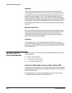
The A3 M/F Power Connector board consists of builtĆin connectors that
distribute the power supply voltages from the A4 Regulator board to the
following boards:
H A1 M/F Strobe Drive board
H A5 Time Base/Controller board
H A26 M/F Acquisition Interconnect board
The A3 M/F Power Connect board also supplies ±15 V power to the A14
Input/Output (I/O) board through a 16Ćpin ribbon cable.
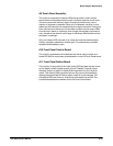
The regulators convert semiĆregulated voltages into stabilized lowĆripple
output voltages. The A4 Regulator board consists of the following regulators
and the voltageĆfault detect circuitry:
H +50 V
H -15 V
H +5 V
H +15 V
H -50 V
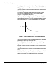
See Figure 9Ć3 for a block diagram of this board.
The operational amplifiers used for the +50 V, +15 V, +5 V, -50 V, -15 V
and -5 V regulators require that the following special voltages be generated
for their operation:
H semiĆregulated +54 V supply generates the +20 V supply
H semiĆregulated -54 V supply generates the -20 V supply
H semiĆregulated +54 V supply generates the +10 V supply
H semiĆregulated -54 V supply generates the -10 V supply
H +10.0 V REF is used as a reference voltage
VoltageĆFault Detect
This circuit consists of two window comparators and associated resistors.
The circuitry detects if any regulated supply is overĆvoltage or underĆvoltage.
The associated resistors set a hysteresis window that is 5% of the regulator
sense line voltages.
A3 M/F Power
Connect Board
A4 Regulator Board