


Product Preview DS21Q55
103 of 248 012103
Please contact telecom.support@dalsemi.com or search http://www.maxim-ic.com for updated
information.
17. CHANNEL BLOCKING REGISTERS
The receive-channel blocking registers (RCBR1/RCBR2/RCBR3/RCBR4) and the transmit-channel
blocking registers (TCBR1/TCBR2/TCBR3/TCBR4) control the RCHBLK and TCHBLK pins,
respectively. The RCHBLK and TCHBLK pins are user-programmable outputs that can be forced high or
low during individual channels. These outputs can be used to block clocks to a USART or LAPD
controller in ISDN–PRI applications. When the appropriate bits are set to a one, the RCHBLK and
TCHBLK pin will be held high during the entire corresponding channel time. Channels 25 through 32 are
ignored when the device is operated in the T1 mode.
Also, the DS21Q55 can internally generate and output a bursty clock on a per-channel basis (N x 64kbps /
56kbps). See Fractional T1/E1 Support.
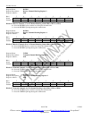
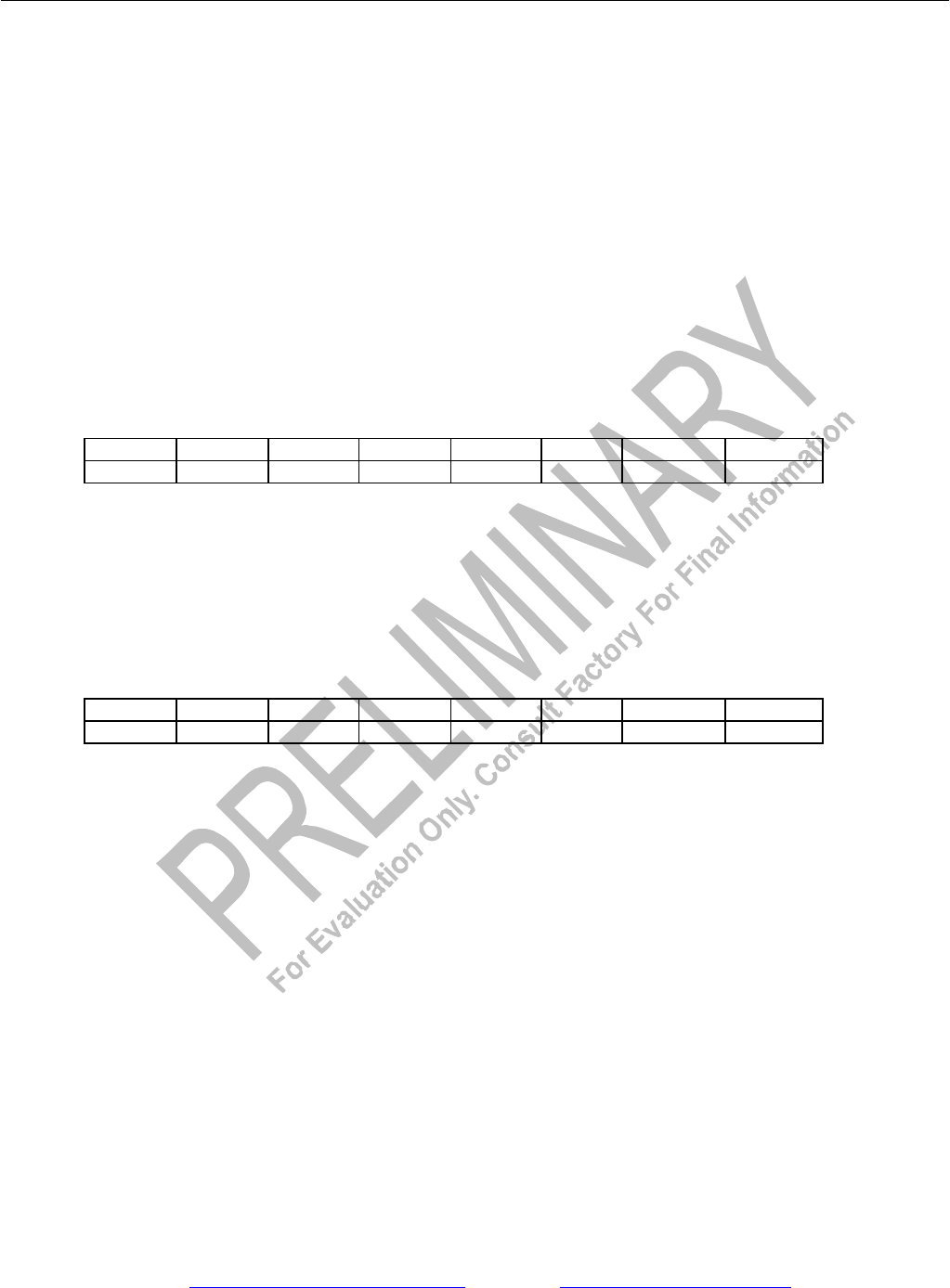
Register Name: RCBR1
Register Description: Receive Channel Blocking Register 1
Register Address: 88h
Bit # 7 6 5 4 3 2 1 0
Name CH8 CH7 CH6 CH5 CH4 CH3 CH2 CH1
Default 0 0 0 0 0 0 0 0
Bits 0 to 7/Receive Channels 1 to 8 Channel Blocking Control Bits (CH1 to CH8).
0 = force the RCHBLK pin to remain low during this channel time
1 = force the RCHBLK pin high during this channel time
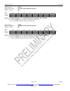
Register Name: RCBR2
Register Description: Receive Channel Blocking Register 2
Register Address: 89h
Bit # 7 6 5 4 3 2 1 0
Name CH16 CH15 CH14 CH13 CH12 CH11 CH10 CH9
Default 0 0 0 0 0 0 0 0
Bits 0 to 7/Receive Channels 9 to 16 Channel Blocking Control Bits (CH9 to CH16).
0 = force the RCHBLK pin to remain low during this channel time
1 = force the RCHBLK pin high during this channel time