


Product Preview DS21Q55
42 of 248 012103
Please contact telecom.support@dalsemi.com or search http://www.maxim-ic.com for updated
information.
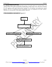
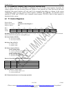
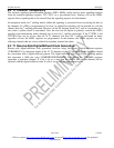
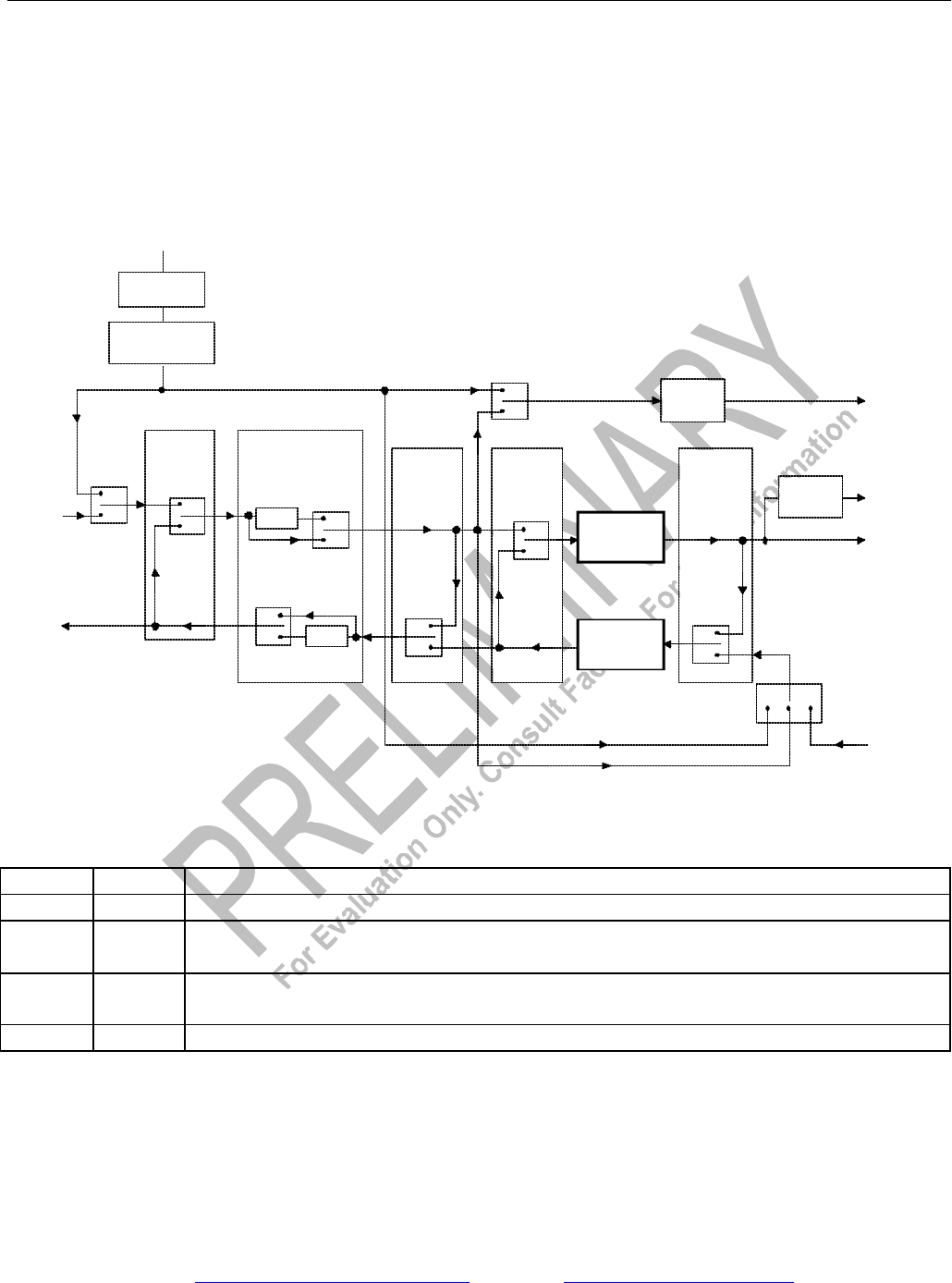
7. CLOCK MAP
Figure 9-1 shows the clock map of the DS21Q55. The routing for the transmit and receive clocks are
shown for the various loopback modes and jitter attenuator positions. Although there is only one jitter
attenuator, which can be placed in the receive or transmit path, two are shown for simplification and
clarity.
CLOCK MAP Figure 9-1
The TCLK MUX is dependent on the state of the TCSS0 and TCSS1 bits in the LIC1 register and the
state of the TCLK pin.
TCSS1 TCSS0 TRANSMIT CLOCK SOURCE
0 0 The TCLK pin (C) is always the source of Transmit Clock.
0 1 Switch to the recovered clock (B) when the signal at the TCLK pin fails to
transition after 1 channel time.
1 0 Use the scaled signal (A) derived from MCLK as the Transmit Clock. The TCLK
pin is ignored.
1 1 Use the recovered clock (B) as the Transmit Clock. The TCLK pin is ignored.
TRANSMIT
FORMATTER
RECEIVE
FRAMER
BPCLK
SYNTH
REMOTE
LOOPBACK
FRAMER
LOOPBACK
PAYLOAD
LOOPBACK
(SEE NOTES)
LTCA
LTCA
JITTER ATTENUATOR
SEE LIC1 REGISTER
LOCAL
LOOPBACK
BPCLK
RCLK
TCLK
MCLK
RXCLK
TXCLK
TO
LIU
LLB = 0
LLB = 1
PLB = 0
PLB = 1
RLB = 1
RLB = 0
FLB = 1
FLB = 0
JAS = 0
AND
DJA = 0
JAS = 1
OR
DJA = 1
JAS = 0
OR
DJA = 1
JAS = 1
AND
DJA = 0
RCL = 1
RCL = 0
DJA = 1
DJA = 0
8XCLK8 x PLL
PRE-SCALER
LIC4.MPS0
LIC4.MPS1
LIC2.3
2.048 TO 1.544
SYNTHESIZER
BA
C
TCLK
MUX