


Product Preview DS21Q55
104 of 248 012103
Please contact telecom.support@dalsemi.com or search http://www.maxim-ic.com for updated
information.
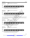
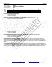
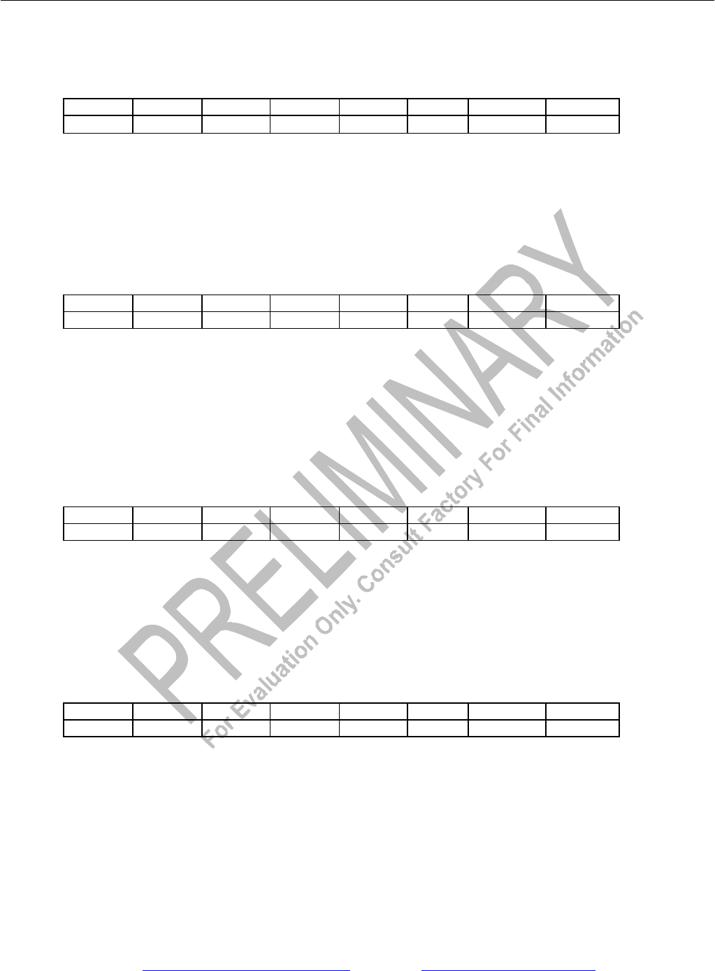
Register Name: RCBR3
Register Description: Receive Channel Blocking Register 3
Register Address: 8Ah
Bit # 7 6 5 4 3 2 1 0
Name CH24 CH23 CH22 CH21 CH20 CH19 CH18 CH17
Default 0 0 0 0 0 0 0 0
Bits 0 to 7/Receive Channels 17 to 24 Channel Blocking Control Bits (CH17 to CH24).
0 = force the RCHBLK pin to remain low during this channel time
1 = force the RCHBLK pin high during this channel time
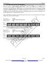
Register Name: RCBR4
Register Description: Receive Channel Blocking Register 4
Register Address: 8Bh
Bit # 7 6 5 4 3 2 1 0
Name CH32 CH31 CH30 CH29 CH28 CH27 CH26 CH25
Default 0 0 0 0 0 0 0 0
Bits 0 to 7/Receive Channels 25 to 32 Channel Blocking Control Bits (CH25 to CH32).
0 = force the RCHBLK pin to remain low during this channel time
1 = force the RCHBLK pin high during this channel time
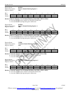
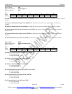
Register Name: TCBR1
Register Description: Transmit Channel Blocking Register 1
Register Address: 8Ch
Bit # 7 6 5 4 3 2 1 0
Name CH8 CH7 CH6 CH5 CH4 CH3 CH2 CH1
Default 0 0 0 0 0 0 0 0
Bits 0 to 7/Transmit Channels 1 to 8 Channel Blocking Control Bits (CH1 to CH8).
0 = force the TCHBLK pin to remain low during this channel time
1 = force the TCHBLK pin high during this channel time
Register Name: TCBR2
Register Description: Transmit Channel Blocking Register 2
Register Address: 8Dh
Bit # 7 6 5 4 3 2 1 0
Name CH16 CH15 CH14 CH13 CH12 CH11 CH10 CH9
Default 0 0 0 0 0 0 0 0
Bits 0 to 7/Transmit Channels 9 to 16 Channel Blocking Control Bits (CH9 to CH16).
0 = force the TCHBLK pin to remain low during this channel time
1 = force the TCHBLK pin high during this channel time