


Product Preview DS21Q55
13 of 248 012103
Please contact telecom.support@dalsemi.com or search http://www.maxim-ic.com for updated
information.
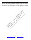
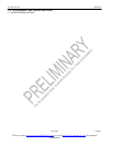
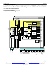
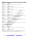
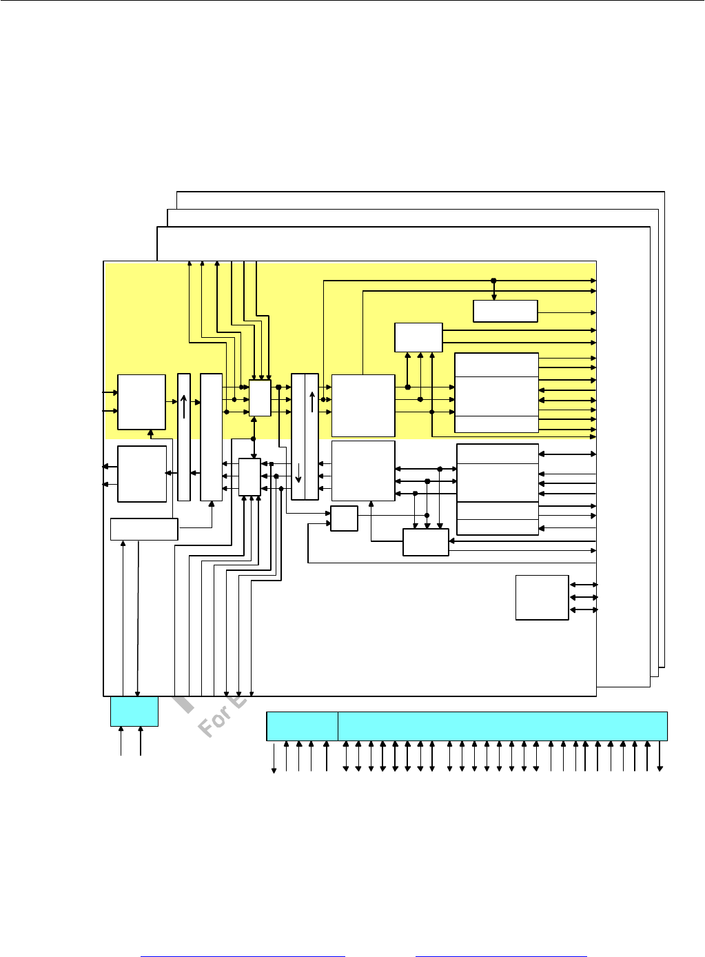
2. BLOCK DIAGRAM
A simplified block diagram showing the major components of the DS21Q55 is shown in Figure 4-1.
Details are shown in subsequent figures. The block diagram is then divided into three functional blocks:
LIU, framer, and backplane interface.
BLOCK DIAGRAM Figure 4-1
Receive Side
Framer
Transmit Side
Formatter
Elastic
Store
TSYNC
TCLK
TCHCLK
TSER
TCHBLK
RCHCLK
RCHBLK
RMSYNC
TSSYNC
TSYSCLK
RSER
RSYSCLK
RSYNC
RFSYNC
TLINK
TLCLK
Timing
Control
Elastic
Store
Sync Control
Timing Control
RLOS/LOTC
Local Loopback
TRING
TTIP
Jitter Attenuator
Either transmit or receive path
Receive
Line I/F
Clock / Data
Recovery
RRING
RTIP
Remote Loopback
VCO / PLL
BPCLK
8.192MHz Clock
Synthesizer
RCLK
Parallel Control Port (routed to all blocks)
D0/AD0
BTS
INT*
WR*(R/W*)
RD*(DS*)
CS1*
TSTRST
A0
MUX
Transmit
Line I/F
DATA
CLOCK
SYNC
Framer Loopback
HDLC/BOC
Controller
LOTC
MUX
HDLC/BOC
Controller
SYNC
CLOCK
DATA
RLINK
RLCLK
TRANSCEIVER #2
TRANSCEIVER #3
TRANSCEIVER #4
D1/AD1
D2/AD2
D3/AD3
D4/AD4
D5/AD5
D6/AD6
D7/AD7
A1
A2
A3
A4
A5
A6
A7/ALE(AS)
MCLK1
Common
MCLK
CS2*
CS3*
CS4*
TPOSO
TNEGO
TCLKO
TPOSI
TNEGI
TCLKI
MUX
MUX
RPOSO
RNEGO
RCLKO
RPOSI
RNEGI
RCLKI
LIUCI
ESIB
ESIBRD
ESIBS0
ESIBS1
Signaling Buffer
TSIG
RSIGF
RSIG
Signaling Buffer
JTAG Port
JTCLK
JTTST
JTMS
JTDI
JTDO
MCLK2