


Product Preview DS21Q55
44 of 248 012103
Please contact telecom.support@dalsemi.com or search http://www.maxim-ic.com for updated
information.
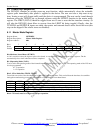
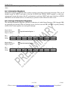
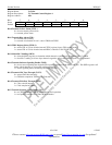
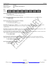
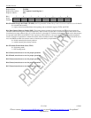
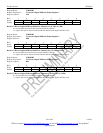
Register Name: T1RCR2
Register Description: T1 Receive Control Register 2
Register Address: 04h
Bit # 7 6 5 4 3 2 1 0
Name - RFM RB8ZS RSLC96 RZSE RZBTSI RJC RD4YM
Default 0 0 0 0 0 0 0 0
Bit 0/Receive Side D4 Yellow Alarm Select (RD4YM).
0 = zeros in bit 2 of all channels
1 = a one in the S-bit position of frame 12 (J1 Yellow Alarm Mode)
Bit 1/Receive Japanese CRC6 Enable (RJC).
0 = use ANSI/AT&T/ITU CRC6 calculation (normal operation)
1 = use Japanese standard JT–G704 CRC6 calculation
Bit 2/Receive Side ZBTSI Support Enable (RZBTSI). Allows ZBTSI information to be output on RLINK pin.
0 = ZBTSI disabled
1 = ZBTSI enabled
Bit 3/Receive FDL Zero Destuffer Enable (RZSE). Set this bit to zero if using the internal HDLC/BOC controller instead of
the legacy support for the FDL. See Legacy FDL Support (T1 Mode) for details.
0 = zero destuffer disabled
1 = zero destuffer enabled
Bit 4/Receive SLC–96 Enable (RSLC96). Only set this bit to a one in SLC–96 framing applications. See D4/SLC–96
Operation for details.
0 = SLC–96 disabled
1 = SLC–96 enabled
Bit 5/Receive B8ZS Enable (RB8ZS).
0 = B8ZS disabled
1 = B8ZS enabled
Bit 6/Receive Frame Mode Select (RFM).
0 = D4 framing mode
1 = ESF framing mode
Bit 7/Unused, must be set to zero for proper operation.