


Product Preview DS21Q55
204 of 248 012103
Please contact telecom.support@dalsemi.com or search http://www.maxim-ic.com for updated
information.
SAMPLE/PRELOAD
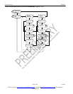
This is a mandatory instruction for the IEEE 1149.1 specification that supports two functions. The digital
I/Os of the device can be sampled at the boundary scan register without interfering with the normal
operation of the device by using the capture-DR state. SAMPLE/PRELOAD also allows the device to
shift data into the boundary scan register via JTDI using the shift-DR state.
BYPASS
When the BYPASS instruction is latched into the parallel instruction register, JTDI connects to JTDO
through the one-bit bypass test register. This allows data to pass from JTDI to JTDO not affecting the
device’s normal operation.
EXTEST
This allows testing of all interconnections to the device. When the EXTEST instruction is latched in the
instruction register, the following actions occur. Once enabled via the Update-IR state, the parallel
outputs of all digital output pins will be driven. The boundary scan register will be connected between
JTDI and JTDO. The Capture-DR will sample all digital inputs into the boundary scan register.
CLAMP
All digital outputs of the device will output data from the boundary scan parallel output while connecting
the bypass register between JTDI and JTDO. The outputs will not change during the CLAMP instruction.
HIGH-Z
All digital outputs of the device will be placed in a high impedance state. The BYPASS register will be
connected between JTDI and JTDO.
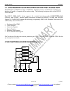
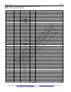
IDCODE
When the IDCODE instruction is latched into the parallel instruction register, the identification test
register is selected. The device identification code will be loaded into the identification register on the
rising edge of JTCLK following entry into the capture-DR state. Shift-DR can be used to shift the
identification code out serially via JTDO. During test-logic-reset, the identification code is forced into the
instruction register’s parallel output. The ID code will always have a 1 in the LSB position. The next 11
bits identify the manufacturer’s JEDEC number and number of continuation bytes followed by 16 bits for
the device and 4 bits for the version (Table 34-2). Table 34-3 lists the device ID codes for the devices.
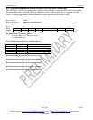
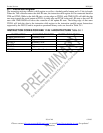
ID CODE STRUCTURE Table 34-2
MSB LSB
Version
Contact Factory
Device ID JEDEC 1
4 bits 16 bits 00010100001 1
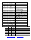
DEVICE ID CODES Table 34-3
DEVICE 16-BIT ID
DS2155 0010h
DS21354 0005h
DS21554 0003h
DS21352 0004h